
Semiconductor light-emitting element

A light-emitting element and semiconductor technology, which is applied in the direction of semiconductor devices, electrical components, electric solid-state devices, etc., can solve problems such as the reduction of luminous efficiency

Active Publication Date: 2021-03-19
EPISTAR CORP
View PDF7 Cites 0 Cited by
  • Summary
  • Abstract
  • Description
  • Claims
  • Application Information

AI Technical Summary

Problems solved by technology

Because the n-type electrode a2 needs enough area to facilitate subsequent manufacturing processes, such as wire bonding, most of the active layer 1106 is removed, resulting in reduced luminous efficiency

Method used


Image

  • Semiconductor light-emitting element
  • Semiconductor light-emitting element
  • Semiconductor light-emitting element

Examples


Embodiment Construction

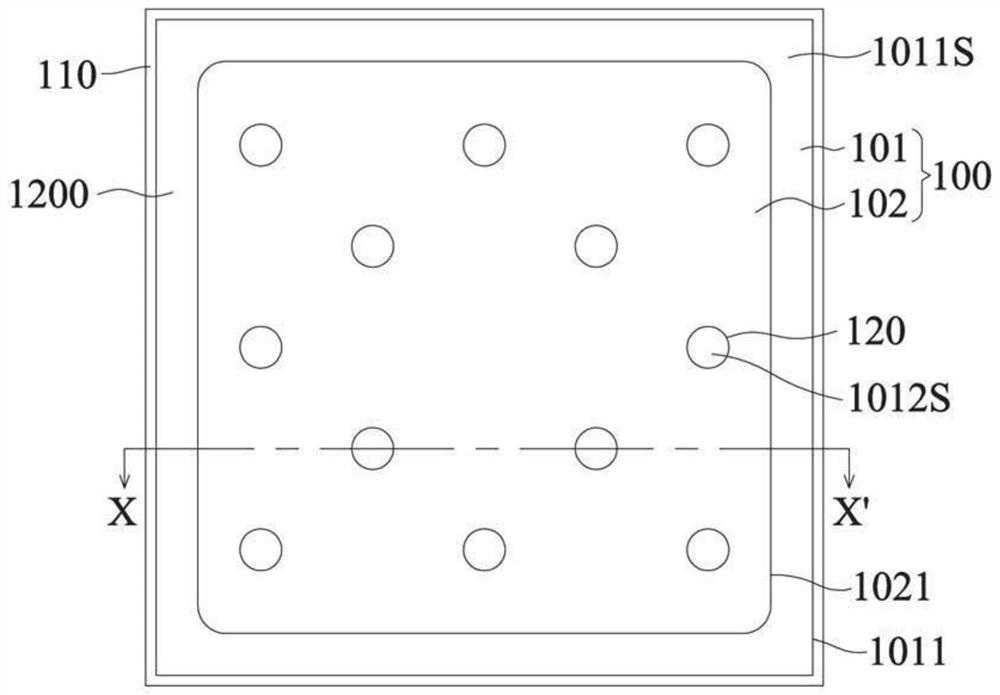
[0071] Figure 3A ~ Figure 10B It is a manufacturing method of the semiconductor light emitting element V according to an embodiment of the present invention. Figure 3A , Figure 4A , Figure 5A , Figure 6A , Figure 7A , Figure 8A , Figure 9A and Figure 10A for the floor plan. Figure 3B , Figure 4B , Figure 5B , Figure 6B , Figure 7B , Figure 8B , Figure 9B , Figure 10B respectively Figure 3A , Figure 4A , Figure 5A , Figure 6A , Figure 7A , Figure 8A , Figure 9A and Figure 10A Sectional view along X-X'.

[0072] Such as Figure 3A and Figure 3B As shown, a semiconductor stack 100 is formed on a growth substrate 110 . The growth substrate 110 may be a sapphire substrate, but is not limited thereto. The semiconductor stack 100 includes a first semiconductor layer 101 , a second semiconductor layer 102 , and an active layer 103 formed between the first semiconductor layer 101 and the second semiconductor layer 102 . Each of the f...


PUM


Abstract

The invention discloses a semiconductor light-emitting element, which comprises a semiconductor stack with a first semiconductor layer, a second semiconductor layer and an active layer; a plurality of first grooves pass through the second semiconductor layer and the active layer to expose the first A semiconductor layer; a second trench passes through the second semiconductor layer and the active layer to expose the first semiconductor layer, wherein the second trench is close to an outermost side of the active layer and surrounds the active layer and a plurality of first trenches; a The patterned metal layer is located on the second semiconductor layer, and in one of the plurality of first trenches or in the second trench; and a first soldering portion and a second soldering portion are located on the second semiconductor layer, and are respectively electrically connected to the second semiconductor layer and the first semiconductor layer.

Description

technical field [0001] The invention relates to a structure of a semiconductor light emitting element. Background technique [0002] Light-emitting diodes (Light-emitting Diodes; LEDs) have been widely used in optical display devices, traffic signs, data storage devices, communication devices, lighting devices and medical equipment. Such as figure 2 As shown, the existing LED has an n-type semiconductor layer 1104, an active layer 1106 and a p-type semiconductor layer 1108 sequentially formed on a substrate 1102, part of the p-type semiconductor layer 1108 and the active layer 1106 are removed to A portion of the n-type semiconductor layer 1104 is exposed, and a p-type electrode a1 and an n-type electrode a2 are respectively formed on the p-type semiconductor layer 1108 and the n-type semiconductor layer 1104 . Since the n-type electrode a2 needs enough area to facilitate the subsequent manufacturing process, such as wire bonding, most of the active layer 1106 is removed, ...

Claims


Application Information

Patent Timeline
Patent Type & Authority Patents(China)
IPC IPC(8): H01L33/38H01L33/62H01L27/15
CPCH01L27/153H01L33/385H01L33/62H01L33/22H01L33/46H01L2224/48091H01L2224/73265H01L33/382H01L2924/00014H01L33/08H01L33/38H01L33/44H01L33/405H01L33/02H01L33/00H01L33/10H01L33/42H01L33/24H01L33/0012H01L33/387
Inventor 陈昭兴王佳琨曾咨耀蒋宗勋胡柏均庄文宏林昱伶
Owner EPISTAR CORP
Learn More