A kind of planar Gunn millimeter wave, terahertz power amplifier and its preparation method
A power amplifier, millimeter wave technology, applied in the direction of bulk negative resistance effect devices, electrical components, circuits, etc., can solve the problem of inability to realize the signal amplification function, and achieve the effect of simple structure and high gain
- Summary
- Abstract
- Description
- Claims
- Application Information
AI Technical Summary
Problems solved by technology
Method used
Image
Examples
Embodiment 1
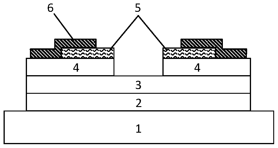
[0048] A planar Gunn millimeter-wave, terahertz power amplifier, such as figure 1 As shown, it includes substrate 1, buffer layer 2, channel layer 3, cap layer 4, ohmic contact electrode 5, and coplanar waveguide electrode 6 from bottom to top. The carrier concentration of channel layer 3 is 8×10 16 cm -3 , the length of the channel layer 3 is 4 μm, and the value of the product N of the carrier concentration of the channel layer 3 and the length of the channel layer 3 is 3.2×10 13 cm -2 .
[0049] The working principle of the planar Gunn power amplifier is that the differential negative resistance in the Gunn effect amplifies the AC signal. The carrier concentration of the channel layer 3 of the device, the length of the channel layer 3 and the product N of the carrier concentration and the length of the channel layer 3 all affect the power amplification performance of the device. An excessively low carrier concentration in the channel layer 3 will lead to an increase in d...
Embodiment 2
[0061] According to a kind of planar Gunn's millimeter wave and terahertz power amplifier described in embodiment 1, the difference is that the length of the channel layer 3 is 2 μm, and the carrier concentration of the channel layer 3 is equal to the length of the channel layer 3 The value of the product N is 1.6×10 13 cm -2 .
Embodiment 3
[0063] According to a kind of planar Gunn millimeter wave and terahertz power amplifier described in embodiment 1, the difference is that the length of the channel layer 3 is 6 μm, and the carrier concentration of the channel layer 3 is equal to the length of the channel layer 3 The value of the product N is 4.8×10 13 cm -2 .
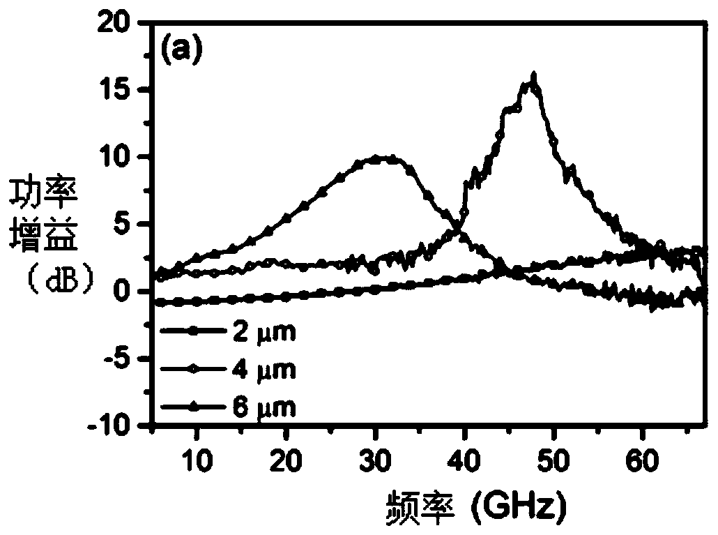
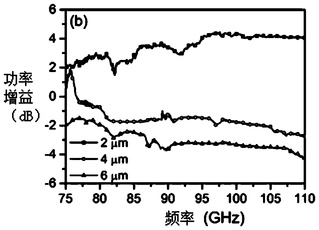
[0064] figure 2 It is a schematic diagram of the power gain test result curves of power amplifiers with channel layer lengths of 2, 4 and 6 μm at frequencies of 6 to 67 GHz; image 3 It is a schematic diagram of the power gain test results curves of power amplifiers with channel layer lengths of 2, 4 and 6 μm at frequencies from 75 to 110 GHz; the peak gain reaches 17 dB, and the highest operating frequency exceeds 110 GHz. It reflects the high frequency and high gain characteristics of the power amplifier.
PUM
| Property | Measurement | Unit |
|---|---|---|
| length | aaaaa | aaaaa |
| thickness | aaaaa | aaaaa |
| thickness | aaaaa | aaaaa |
Abstract
Description
Claims
Application Information


