Packaging structure, packaging method and photoelectric equipment

A packaging structure and packaging method technology, applied in the direction of circuits, electrical components, electrical solid devices, etc., can solve problems such as poor water vapor sealing effect, and achieve the effect of improving utilization

Active Publication Date: 2018-03-20
NANJING TECH CORP LTD
View PDF4 Cites 10 Cited by
  • Summary
  • Abstract
  • Description
  • Claims
  • Application Information

AI Technical Summary

Problems solved by technology

[0004] The main purpose of the present invention is to provide a packaging structure, packaging method and optoelectronic equipment to solve the problem of poor sealing effect on water vapor in the packaging structure of light-emitting devices in the prior art

Method used


Image

  • Packaging structure, packaging method and photoelectric equipment
  • Packaging structure, packaging method and photoelectric equipment
  • Packaging structure, packaging method and photoelectric equipment

Examples


preparation example Construction

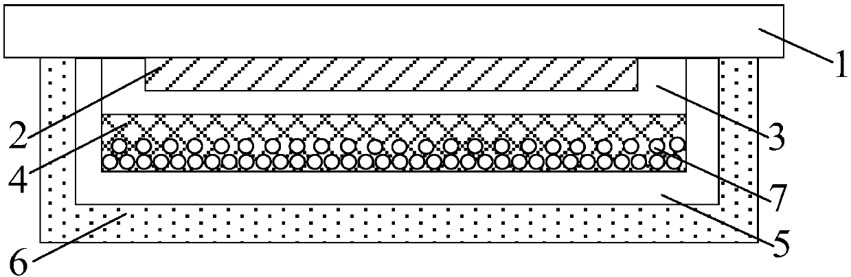
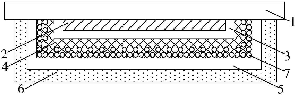
[0082] The preparation temperature of the above-mentioned second water-absorbing layer varies according to different preparation methods. For example, when the chemical vapor deposition method is used, the temperature is generally above 130° C., and the vacuum evaporation method is generally used. The manufacturing temperature is between 25 and 40° C., while The production temperature of atomic layer deposition is generally between 60 and 100 ° C. Among them, the preparation temperature of vacuum evaporation method and atomic layer deposition method is within the tolerance temperature range of light-emitting devices, and will not have high temperature effects on light-emitting devices. Chemical vapor phase Even if the temperature of the second water-absorbing layer prepared by the deposition method exceeds the tolerance temperature range of the light-emitting device, its heat will be blocked by the reticular void layer and will not affect the light-emitting device. The function ...

Embodiment 1

[0090]The specific packaging process is in a class 100 clean room. The specific packaging methods include:

[0091] First, prepare an ITO (indium tin oxide) flexible substrate, and prepare a light-emitting device on the ITO flexible substrate. The light-emitting device includes a hole injection layer prepared on the surface of the ITO (the material is poly(3,4-ethylenedioxythiophene)- Polystyrene sulfonic acid, PEDOT:PSS), prepare hole transport layer (material is polyvinyl carbazole PVK) on hole injection layer upper surface, the quantum dot light-emitting layer on hole transport layer surface (material is CdSe / ZnS core-shell quantum dots), and an electron transport layer (ZnO nanoparticles) on the surface of the quantum dot light-emitting layer, and a cathode (material is Ag) on ​​the electron transport layer.

[0092] Then, coat a layer of copper oxide nanoparticle ink on the cathode surface of the light-emitting device and other surfaces of the light-emitting device that...

Embodiment 2

[0098] The specific packaging process is in a class 100 clean room. The specific packaging methods include:

[0099] First, an ITO flexible substrate is prepared, and a light-emitting device is fabricated on the ITO flexible substrate, and this step is the same as that of the above-mentioned embodiment 1.

[0100] Then, forming a pre-resistance liquid layer, this step is the same as the above-mentioned embodiment 1;

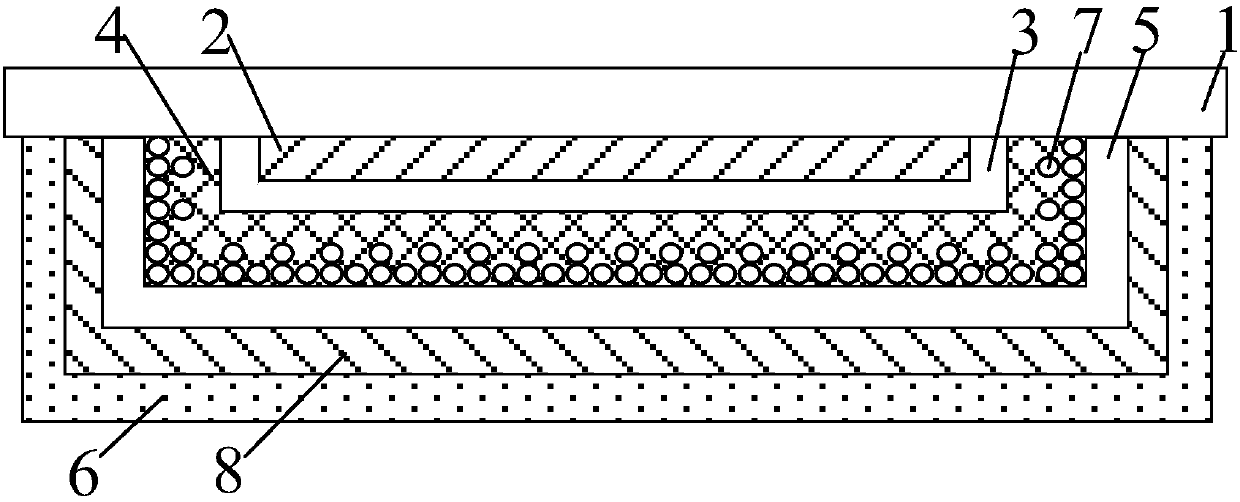
[0101] Coat a layer of ketone airgel solution on the pre-resistance liquid layer, its solvent mainly includes methyl ethyl ketone, use coating and printing equipment to make ketone airgel, and then use low critical drying process to process it , dry at a drying temperature of 85°C and a critical pressure of 3Mpa for 5 minutes to prepare the pre-void layer, and sinter the upper pre-void layer and the pre-resistance layer together with a xenon lamp to form a reticular void layer and a liquid-resistance layer. The thickness of each layer is 2 μm and 30 nm, respect...


PUM


Abstract

The invention provides a packaging structure, a packaging method and photoelectric equipment. The packaging structure comprises a substrate, a light emitting device, a liquid blocking layer, a net-shaped gap layer, a first water absorbing layer and at least one sealing barrier layer, wherein the light emitting device is arranged on one side surface of the substrate; the liquid blocking layer is arranged on the exposed surface of the light emitting device; the net-shaped gap layer is arranged on the surface, far from the substrate, of the liquid blocking layer; the material of the net-shaped gap layer comprises aerogel; the first water absorbing layer is arranged on the surface, far from the liquid blocking layer, of the net-shaped gap layer, and connected with the substrate in a sealing manner; the at least one sealing barrier layer is connected with the substrate in a sealing manner to form a sealed space; and the first water absorbing layer, the net-shaped gap layer, the liquid blocking layer and the light emitting device are arranged in the sealed space. By virtue of the packaging structure, the problem of poor sealing effect on vapor of the packaging structure of the light emitting device in the prior art is solved, the light emitting device is effectively protected from external vapor erosion, and the sealing effect is improved.

Description

technical field [0001] The invention relates to the technical field of packaging, in particular to a packaging structure, a packaging method and an optoelectronic device. Background technique [0002] Realizing flexible display is considered to be an important direction in the development of display technology. However, as far as the current conditions are concerned, the industrialization of flexible displays still faces many challenges. These challenges mainly include: how to prepare thin film transistors with high performance and high reliability at low temperature, how to prepare flexible electrodes, and how to develop flexible electroluminescence technology. Devices are effectively encapsulated in thin films, etc. Among them, as people have higher and higher requirements on the quality and lifespan of flexible electroluminescent devices, how to eliminate the main factor affecting the quality and lifespan of the package—water vapor has become an issue that people pay mor...

Claims


Application Information

Patent Timeline
Patent Type & Authority Applications(China)
IPC IPC(8): H01L51/52
CPCH01L21/56H01L23/29H01L23/3107H10K50/846H10K50/844
Inventor 王兵甄常刮
Owner NANJING TECH CORP LTD
Why Eureka
Try Eureka