Binary optical filter and manufacture method thereof

A manufacturing method and filter technology, applied in the field of optical filters, can solve the problems of photoresist 300 denaturation, reducing the yield of integrated filter samples, difficult to control accurately, etc., and achieve the effect of overcoming the problem of residual glue

Active Publication Date: 2018-04-03
SUZHOU INST OF NANO TECH & NANO BIONICS CHINESE ACEDEMY OF SCI
View PDF6 Cites 5 Cited by
  • Summary
  • Abstract
  • Description
  • Claims
  • Application Information

AI Technical Summary

Problems solved by technology

[0003] The above method will adversely affect the performance of the first filter film in the process of patterning the second filter film
refer to Figure 1-Figure 2 , when the photolithographic lift-off process is used to prepare the integrated optical filter, after the patterning of the first optical filter film 210 on the substrate 100 is completed, the first optical filter film 210 needs to be covered with photoresist 300 to play a protective role, and then Preparation of the second filter film 220, the second filter film 220 will be in a high temperature state for a long time during the preparation process, and accompanied by ion beam bombardment, resulting in denaturation of the photoresist 300, which is difficult to remove, so that There is residual glue 300a on the surface of the first filter film 210 (such as figure 2 ), thereby causing the performance of the first filter film 210 to decline, reducing the yield of the entire integrated filter sample
or refer to Figure 3-Figure 5 , when the integrated optical filter is prepared by etching process, after the patterning of the first optical filter film 210 on the substrate 100 is completed, the second optical filter film 220 is directly prepared, so it is difficult to precisely control the The second filter film 220 is etched clean, which is easy to cause over-etching (such as Figure 4 ) or not completely etched (such as Figure 5 ) problem, causing the first filter film 210 to be thinned or leaving part of the second filter film 220 on the surface of the first filter film 210, which will also cause the performance of the first filter film 210 to decline

Method used


Image

  • Binary optical filter and manufacture method thereof
  • Binary optical filter and manufacture method thereof
  • Binary optical filter and manufacture method thereof

Examples


Embodiment Construction

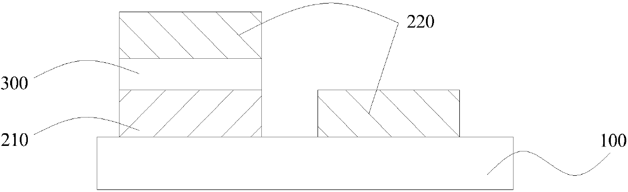
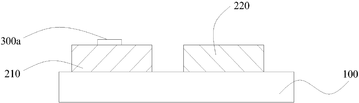
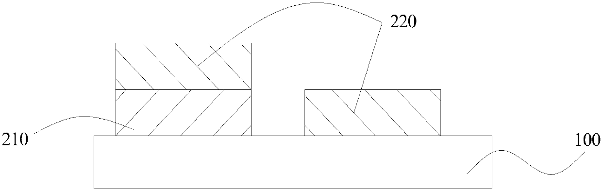
[0023] Hereinafter, embodiments of the present invention will be described in detail with reference to the accompanying drawings. This invention may, however, be embodied in many different forms and should not be construed as limited to the specific embodiments set forth herein. Rather, the embodiments are provided to explain the principles of the invention and its practical application, thereby enabling others skilled in the art to understand the invention for various embodiments and with various modifications as are suited to particular intended uses. In the drawings, the shapes and dimensions of elements may be exaggerated for clarity, and the same reference numerals will be used throughout to designate the same or like elements.

[0024] It will be understood that, although the terms "first", "second", etc. may be used herein to describe various elements, these elements should not be limited by these terms. These terms are only used to distinguish one element from another...


PUM


Abstract

The invention discloses a binary optical filter. The binary optical filter includes a substrate, and a plurality of first filtering units and a plurality of second filtering units in array arrangementon two opposite surfaces of the substrate, wherein projections of the first filtering units and the second filtering units on the first surface or the second surface are distributed in a staggered manner. According to the invention, the binary optical filter has different optical filtering functions and can be combined to a mini-size optical detection system so as to apply to fields including medical diagnosis, atmosphere, space, ocean and the like. The invention also discloses a manufacture method of the above binary optical filter. The manufacture method includes selecting the substrate; forming the first filtering units and the second filtering units on two opposite surfaces of the substrate in array arrangement, wherein the projections of the first filtering units and the second filtering units on the first surface or the second surface are distributed in a staggered manner. According to the invention, simple technique and high integration level are achieved.

Description

technical field [0001] The invention belongs to the technical field of optical filters, and in particular relates to a binary filter and a manufacturing method thereof. Background technique [0002] In order to adapt to the miniaturization of optoelectronic instruments, thin-film optical filters are also developing in the direction of smaller size and higher integration, and the preparation technology is becoming more and more challenging. At present, in the production of integrated optical filters, semiconductor micro-nano processing technology is mostly used, and the first optical filter film is patterned on the surface of the substrate by photolithography or etching technology, and then the second optical filter film is prepared, and repeated In the above patterning step, array patterns with different light filtering functions are arranged on the same surface. [0003] In the above method, the performance of the first filter film will be adversely affected during the pat...

Claims


Application Information

Patent Timeline
Patent Type & Authority Applications(China)
IPC IPC(8): G02B5/20
CPCG02B5/201
Inventor 邢政时文华杨磊姬荣坤
Owner SUZHOU INST OF NANO TECH & NANO BIONICS CHINESE ACEDEMY OF SCI
Why Eureka
Try Eureka