
Encapsulation structure and encapsulation method of optical fingerprint chip

A fingerprint chip and packaging structure technology, applied in the direction of acquiring/organizing fingerprints/palmprints, instruments, electrical components, etc., can solve the problem of low fingerprint recognition accuracy, and achieve the effect of improving accuracy and avoiding crosstalk.

Active Publication Date: 2018-04-17
CHINA WAFER LEVEL CSP
View PDF10 Cites 3 Cited by
  • Summary
  • Abstract
  • Description
  • Claims
  • Application Information

AI Technical Summary

Problems solved by technology

The accuracy of fingerprint recognition in the packaging structure of the existing optical fingerprint chip is low

Method used


Image

  • Encapsulation structure and encapsulation method of optical fingerprint chip
  • Encapsulation structure and encapsulation method of optical fingerprint chip
  • Encapsulation structure and encapsulation method of optical fingerprint chip

Examples


Embodiment Construction

[0075] The following will clearly and completely describe the technical solutions in the embodiments of the present invention with reference to the accompanying drawings in the embodiments of the present invention. Obviously, the described embodiments are only some, not all, embodiments of the present invention. Based on the embodiments of the present invention, all other embodiments obtained by persons of ordinary skill in the art without making creative efforts belong to the protection scope of the present invention.

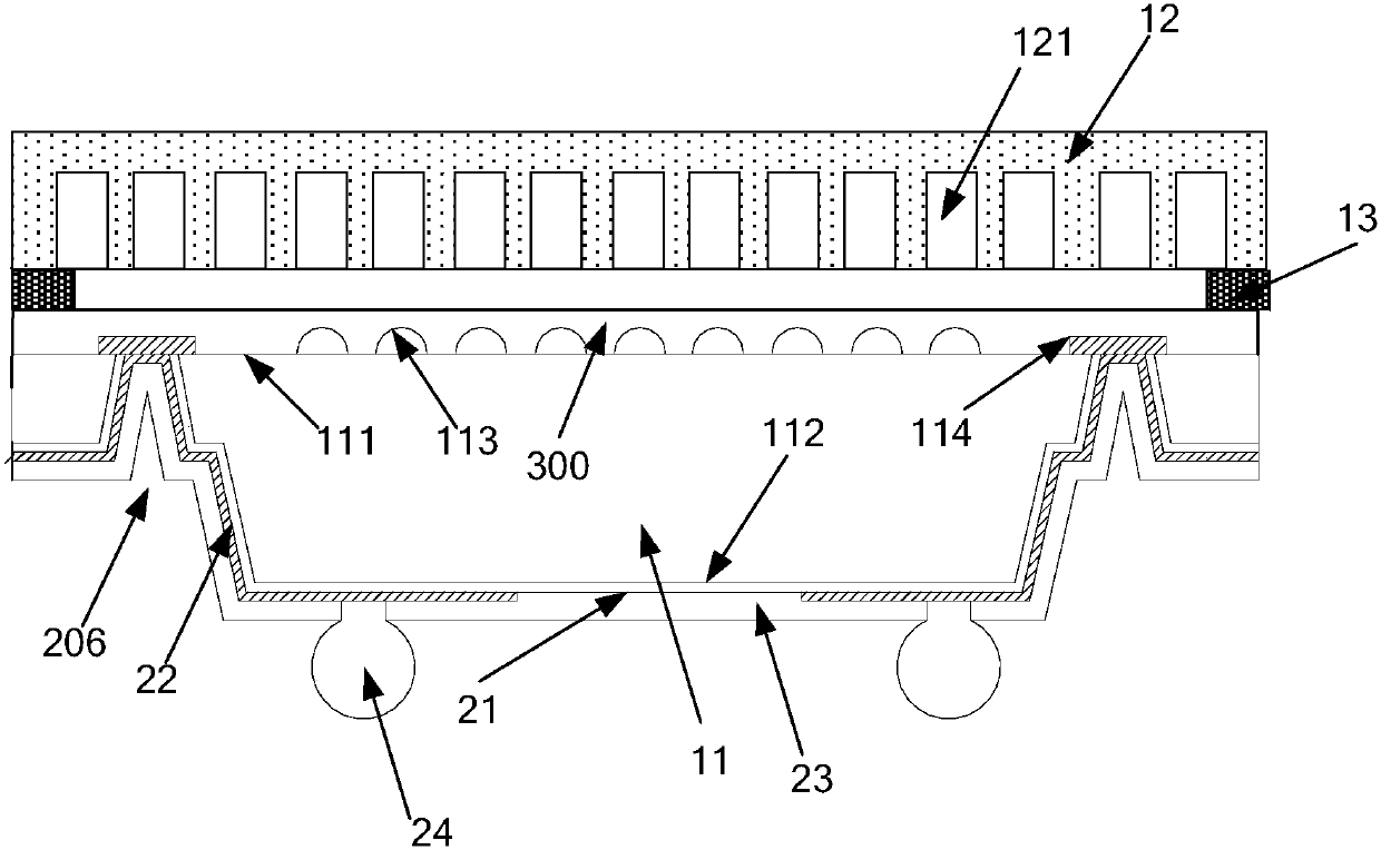
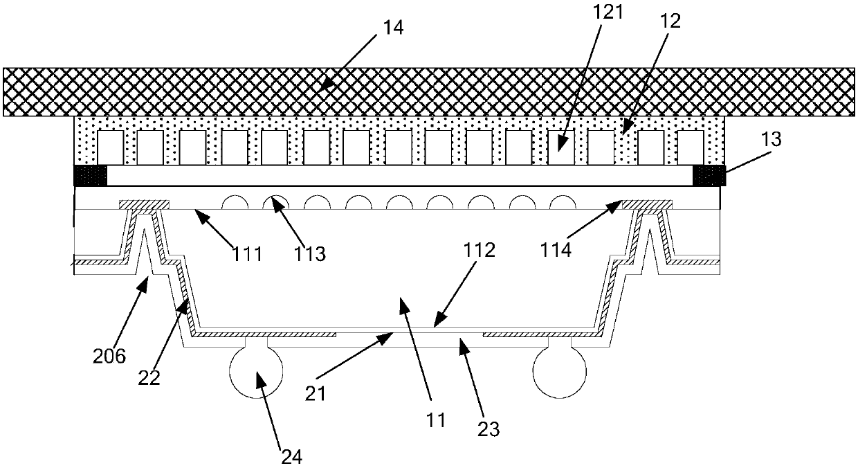
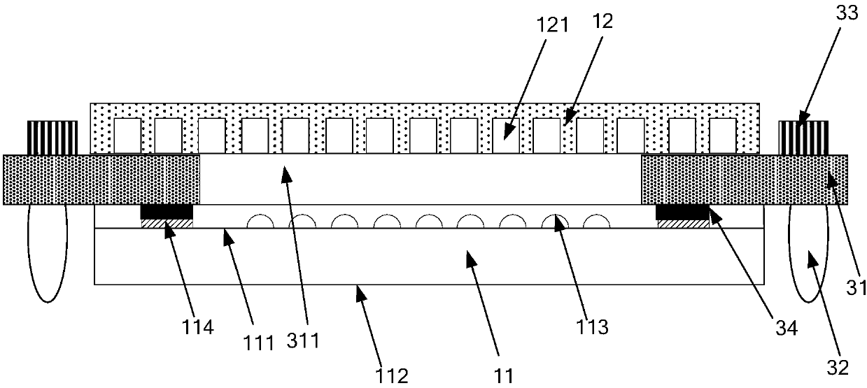
[0076] At present, when the optical fingerprint chip is packaged, a transparent cover plate is generally arranged directly on the front side of the optical fingerprint chip to package and protect the photosensitive pixel unit on the front side. There is a filter between the transparent cover plate and the photosensitive chip. to filter out stray light. However, this method cannot avoid the problem of crosstalk between different photosensitive pixels.

[0077]...


PUM


Abstract

The invention discloses an encapsulation structure and encapsulation method of an optical fingerprint chip. According to the technical scheme, a substrate opposite to the front surface of the opticalfingerprint chip is arranged, the substrate is provided with a photoconductive area corresponding to a photosensitive area, the photoconductive area comprises multiple blind holes, and the depth of the blind holes is smaller than the thickness of the substrate; the position of the photoconductive area is corresponding to that of the photosensitive area. On one hand, the substrate is made of an infrared light-transmittable material, and through the blind holes not running through the substrate, the substrate can be reused as an optical filter and used for filtering out the other stray light except infrared light; on the other hand, through the pinhole imaging effect of the blind holes, optical path adjusting control can be conducted on the incident infrared light, so that the infrared lightat a specific incident angle illuminates corresponding photosensitive pixels, the problem of crosstalk among different photosensitive pixels is avoided, and the accuracy of fingerprint recognition isimproved.

Description

technical field [0001] The invention relates to the technical field of chip packaging, and more specifically, relates to a packaging structure and a packaging method of an optical fingerprint chip. Background technique [0002] With the continuous advancement of science and technology, more and more electronic devices are widely used in people's daily life and work, which brings great convenience to people's daily life and work, and has become an indispensable tool for people today. . With the increasing functions of electronic devices, more and more important information is stored in electronic devices, and the identity verification technology of electronic devices has become a main direction of research and development of electronic devices. [0003] Due to the uniqueness and invariance of fingerprints, fingerprint identification technology has many advantages such as good security, high reliability and simple use. Therefore, fingerprint identification technology has bec...

Claims


Application Information

Patent Timeline
IPC IPC(8): H01L23/31H01L25/065G06K9/00H01L23/498
CPCH01L23/498H01L25/065H01L23/3114G06V40/1341G06V40/12H01L2224/11
Inventor 王之奇谢国梁胡汉青
Owner CHINA WAFER LEVEL CSP
Features
  • Generate Ideas
  • Intellectual Property
  • Life Sciences
  • Materials
  • Tech Scout
  • Unparalleled Data Quality
  • Higher Quality Content
  • 60% Fewer Hallucinations
Learn More