Array substrate, liquid crystal display device and driving method

A liquid crystal display device and array substrate technology, which is applied to static indicators, instruments, nonlinear optics, etc., can solve the problems of different vertical electric field voltage differences, inconsistent brightness of two adjacent pixel units, and uneven brightness and darkness, and achieves a solution to the problem. Uneven brightness and darkness, improve display quality, and improve the effect of inconsistent brightness

Active Publication Date: 2020-07-28
KUSN INFOVISION OPTOELECTRONICS
View PDF4 Cites 0 Cited by
  • Summary
  • Abstract
  • Description
  • Claims
  • Application Information

AI Technical Summary

Problems solved by technology

[0006] like image 3 As shown, in order to invert the display, the polarities of the data voltages applied to two adjacent pixel units are different. The voltage difference is different, so that the vertical electric field voltage difference generated by two adjacent pixel units with different positive and negative polarities is different, resulting in inconsistent brightness of the adjacent two pixel units, and there is a phenomenon of uneven brightness and darkness, such as Figure 4 As shown, the pixel cells on the left are darker than the pixel cells on the right

Method used


Image

  • Array substrate, liquid crystal display device and driving method
  • Array substrate, liquid crystal display device and driving method
  • Array substrate, liquid crystal display device and driving method

Examples


no. 1 example

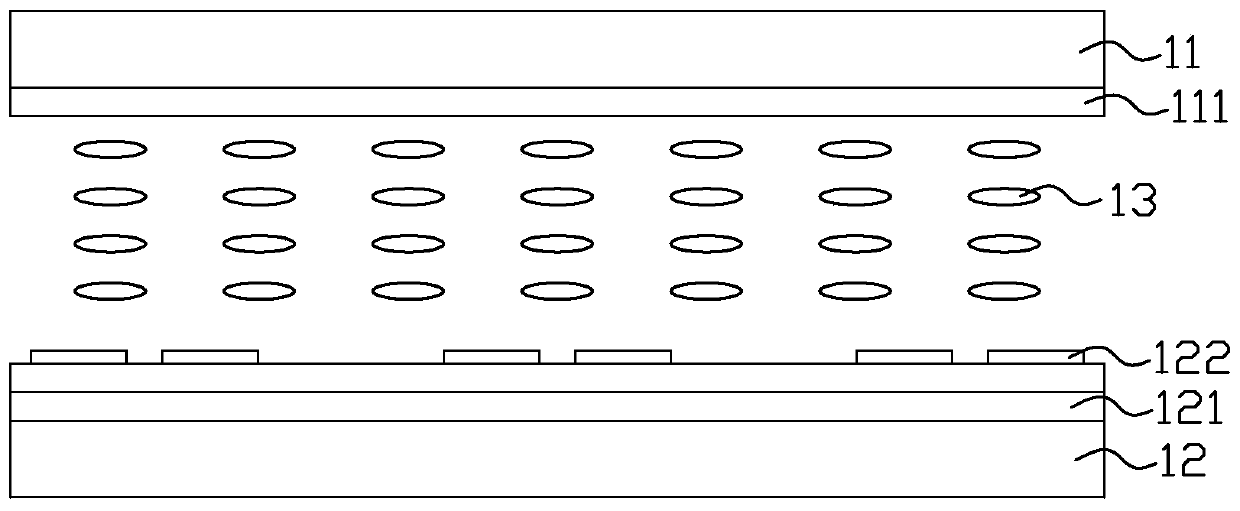
[0034] Please refer to Figure 5 and Figure 6 , the first embodiment of the present invention provides an array substrate 20, the array substrate 20 is provided with a plurality of scanning lines 21, a plurality of data lines 22, a plurality of pixel electrodes 23, a plurality of common electrode strips 24 and a plurality of thin film transistors 26.

[0035] The plurality of scan lines 21 and the plurality of data lines 22 are insulated and intersect to define a plurality of pixel units P arranged in an array, and each pixel unit P is defined by two scan lines 21 and two data lines 22 .

[0036] Each pixel unit P is provided with a thin film transistor 26 and a pixel electrode 23 , and the pixel electrode 23 is connected to the scanning line 21 and the data line 22 adjacent to the thin film transistor 26 through the thin film transistor 26 . Specifically, the thin film transistor 26 includes a gate, an active layer, a source and a drain, wherein the gate is electrically co...

no. 2 example

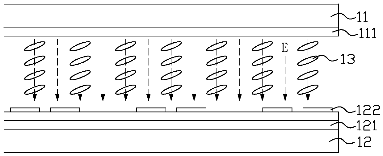
[0040] Such as Figure 7 As shown, the second embodiment of the present invention provides a liquid crystal display device. The liquid crystal display device includes a display panel 50. The display panel 50 includes the above-mentioned array substrate 20, a color filter substrate 30 disposed opposite to the array substrate 20, and a color filter substrate located in the array substrate. The liquid crystal layer 40 between the substrate 20 and the color filter substrate 30 .

[0041] In this embodiment, on the array substrate 20, the plurality of pixel electrodes 23 and the plurality of common electrode blocks 25 are located on different layers with an insulating layer 29 interposed therebetween, so that the liquid crystal display device using the array substrate 20 It may be formed as a fringe field switching type (Fringe Field Switching, FFS). When the liquid crystal display device displays normally, a fringe electric field is generated between the common electrode block 25...

no. 3 example

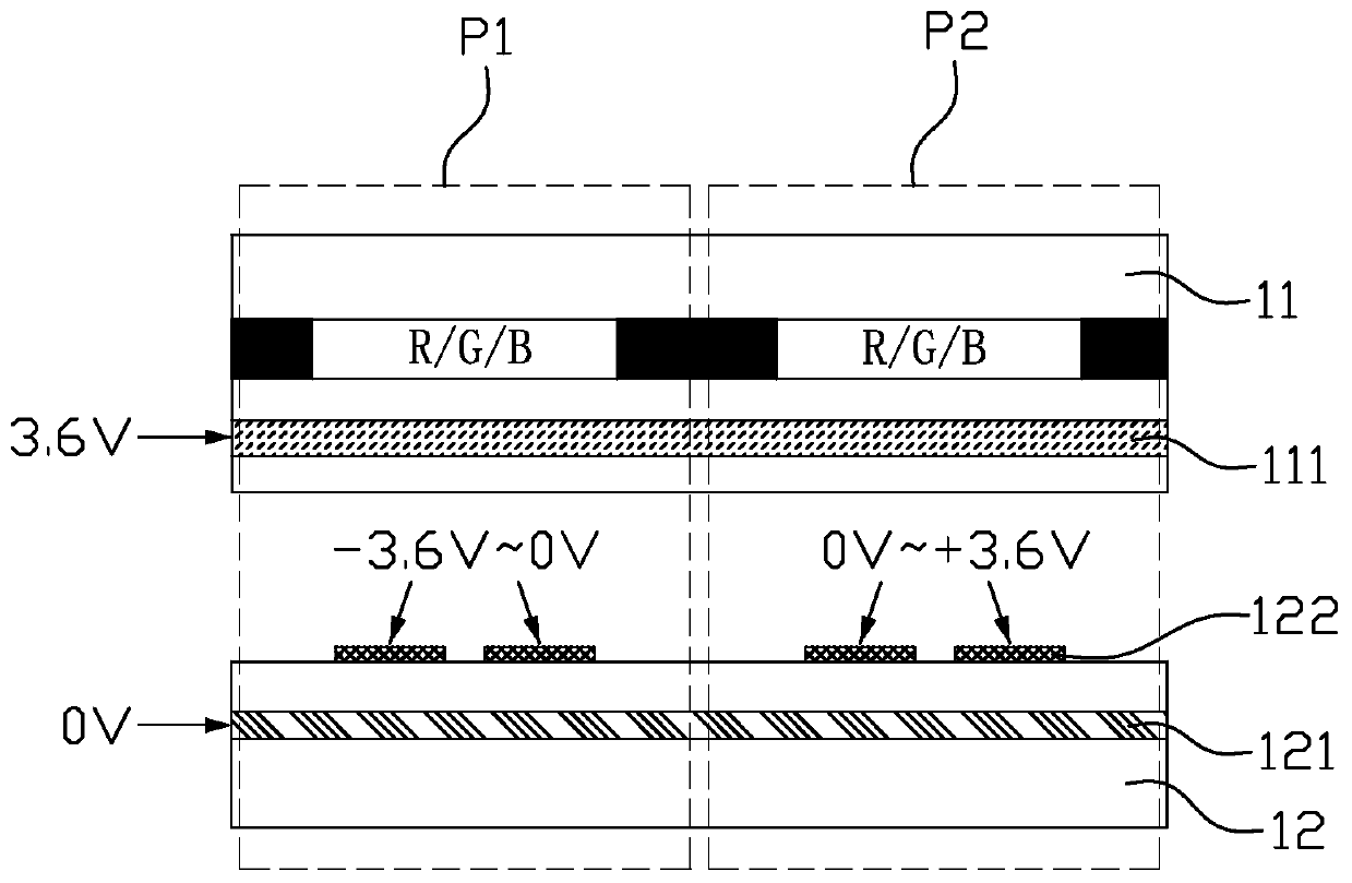
[0057] Please refer to Figure 13 and Figure 14 The difference between the liquid crystal display device provided in this embodiment and the second embodiment above is that the liquid crystal layer 40 in this embodiment uses negative liquid crystal molecules. With the advancement of technology, the performance of negative liquid crystal has been significantly improved, and its application has become more and more extensive. In this example, if Figure 13 As shown, in the initial state (that is, the situation where no voltage is applied to the liquid crystal display device), the negative liquid crystal molecules in the liquid crystal layer 40 have a relatively large initial pretilt angle with respect to the substrates 20 and 30, that is, the negative liquid crystal molecules in the initial state The state is an inclined posture with respect to the substrates 20 , 30 .

[0058] Narrow viewing angle mode: please refer to Figure 13In the liquid crystal display device of this...


PUM


Abstract

Provided are an array substrate, a liquid crystal display device and a driving method. The array substrate is provided with a plurality of scanning lines, a plurality of data lines, a plurality of pixel units and a plurality of common electrode bars. The common electrode bars extend along the direction of the data lines and are spaced apart from each other in the direction of the scanning lines, each common electrode bar is formed by a plurality of common electrode blocks connected in series and arranged in a Z shape, each common electrode block corresponds to one pixel unit, the common electrode bars at odd-numbered positions in the direction of the scanning lines are connected together through a first voltage input line, and the common electrode bars at even-numbered positions in the direction of the scanning lines are connected together through a second voltage input line. According to the liquid crystal display device, the phenomenon of uneven brightness of screen display can be improved while achieving visual angle switching.

Description

technical field [0001] The invention relates to the technical field of liquid crystal display, in particular to an array substrate, a liquid crystal display device and a driving method. Background technique [0002] Liquid crystal display (liquid crystal display, LCD) has the advantages of good image quality, small size, light weight, low driving voltage, low power consumption, no radiation and relatively low manufacturing cost, and occupies a dominant position in the field of flat panel display. [0003] With the continuous advancement of liquid crystal display technology, the viewing angle of the display has been expanded from about 120° to more than 160°. While enjoying the visual experience brought by the large viewing angle, people also hope to effectively protect commercial secrets and personal privacy. Avoid commercial loss or embarrassment caused by information leakage on the screen. Therefore, in addition to a wide viewing angle, it is also required that the displa...

Claims


Application Information

Patent Timeline
Patent Type & Authority Patents(China)
IPC IPC(8): G02F1/1343G02F1/1362G09G3/36G02F1/13
CPCG02F1/1323G02F1/134309G02F1/136286G09G3/36
Inventor 柯中乔
Owner KUSN INFOVISION OPTOELECTRONICS
Why Eureka
Try Eureka