Array substrate, liquid crystal display device and driving method

An array substrate and column pixel technology, applied in the field of liquid crystal display, can solve the problems of doubling, cost increase, power consumption increase, etc., and achieve the effect of improving resolution and improving brightness inconsistency

Active Publication Date: 2020-06-05
KUSN INFOVISION OPTOELECTRONICS
View PDF6 Cites 0 Cited by
  • Summary
  • Abstract
  • Description
  • Claims
  • Application Information

AI Technical Summary

Problems solved by technology

In order to solve the flickering problem of the panel, it is necessary to use a driving circuit with a frame frequency of 120Hz, so that the driving frequency is higher than the human eye recognition frequency, so as to improve the flickering. times, the power consumption increases, and the cost will also increase

Method used


Image

  • Array substrate, liquid crystal display device and driving method
  • Array substrate, liquid crystal display device and driving method
  • Array substrate, liquid crystal display device and driving method

Examples


no. 1 example

[0035] Please refer to Figure 3 to Figure 6 The liquid crystal display device provided by the first embodiment of the present invention includes an array substrate 20 , a color filter substrate 30 disposed opposite to the array substrate 20 , and a liquid crystal layer 40 located between the array substrate 20 and the color filter substrate 30 .

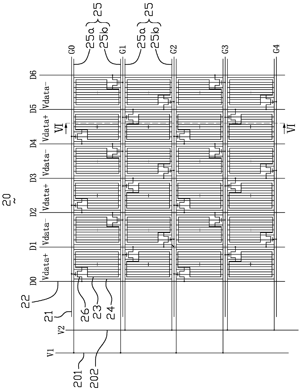
[0036] A plurality of scan lines 21 and a plurality of data lines 22 are disposed on the array substrate 20 . The plurality of scan lines 21 and the plurality of data lines 22 are insulated and intersect to define a plurality of pixel units arranged in an array. Each pixel unit is provided with a pixel electrode 23 , a common electrode 24 and a thin film transistor 26 , and the pixel electrode 23 is connected to the scanning line 21 and the data line 22 adjacent to the thin film transistor 26 through the thin film transistor 26 . Specifically, the thin film transistor 26 includes a gate, a source and a drain, wherein the gate is el...

no. 2 example

[0057] Please refer to Figure 10 The difference between the liquid crystal display device provided in this embodiment and the above-mentioned first embodiment is that in this embodiment, there is only one first conductive strip 25 connected to the common electrode 24 in each row of pixel units, which is located in the row of pixels the underside of the unit. For other structures of this embodiment, reference may be made to the foregoing first embodiment, and details are not repeated here.

no. 3 example

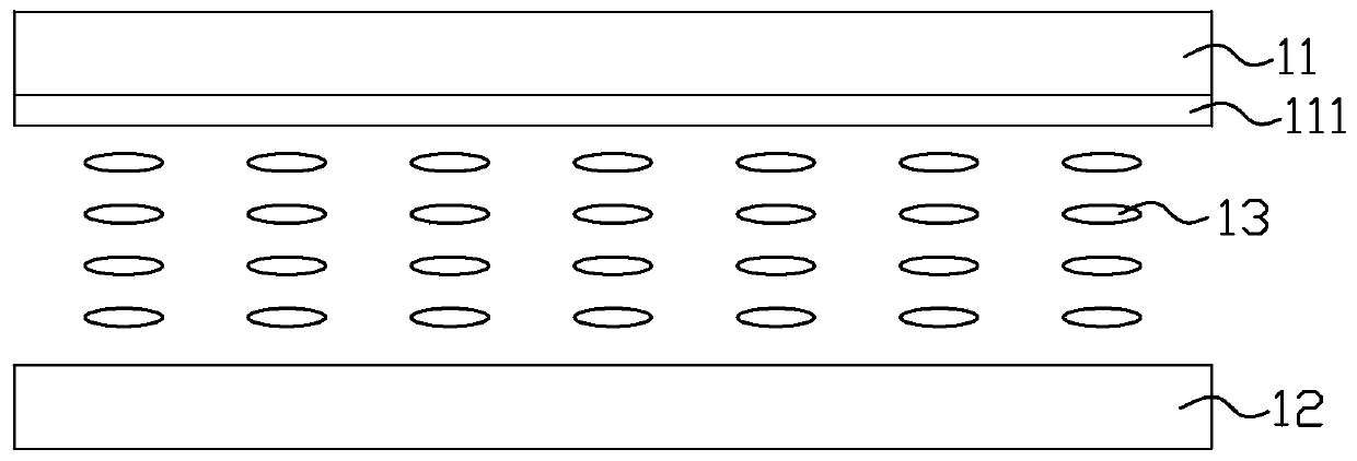
[0059] Please refer to Figure 11 and Figure 12The difference between the liquid crystal display device provided in this embodiment and the first embodiment above is that the liquid crystal layer 40 in this embodiment uses negative liquid crystal molecules. With the advancement of technology, the performance of negative liquid crystal has been significantly improved, and its application has become more and more extensive. In this example, if Figure 11 As shown, in the initial state (that is, the situation where no voltage is applied to the liquid crystal display device), the negative liquid crystal molecules in the liquid crystal layer 40 have a relatively large initial pretilt angle with respect to the substrates 20 and 30, that is, the negative liquid crystal molecules in the initial state The state is an inclined posture with respect to the substrates 20 , 30 .

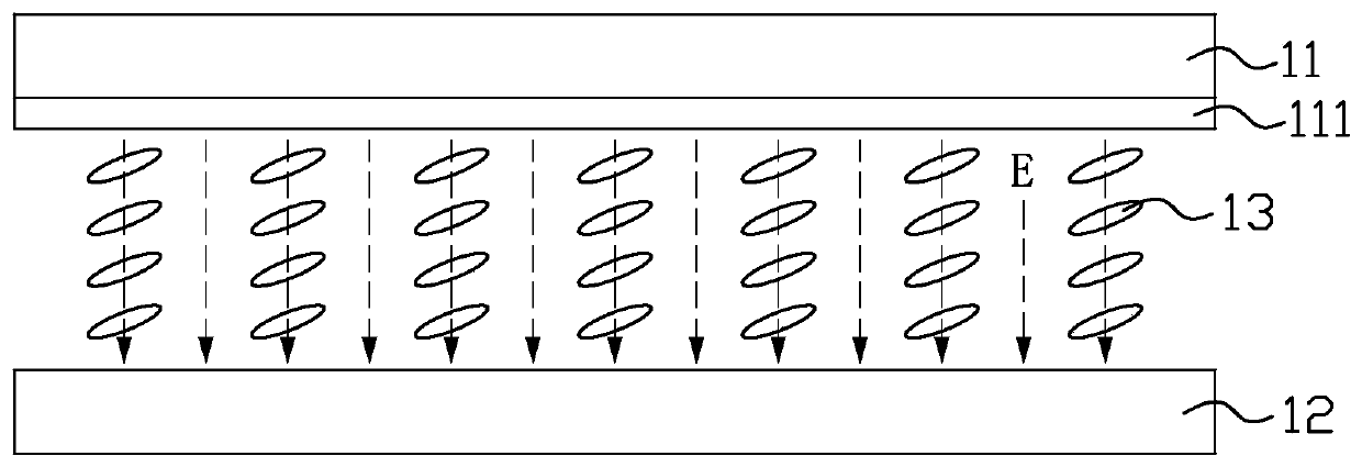
[0060] Narrow viewing angle mode: please refer to Figure 11 In this embodiment, in the narrow viewing ang...


PUM


Abstract

The invention discloses an array substrate, a liquid crystal display device and a driving method. The array substrate is provided with a plurality of scanning lines, a plurality of data lines, a plurality of pixel electrodes, a plurality of common electrodes, a plurality of first conductive strips, a plurality of thin film transistors, a first voltage line and a second voltage line; a pixel electrode and a common electrode are arranged in each pixel unit; the first conductive strips extend in the scanning line direction and are located on the upper sides of the corresponding scanning lines tooverlap the scanning lines, and the common electrodes in each row of pixel units are connected to the same first conductive strip; the first conductive strips are alternately connected to the first voltage line and the second voltage line in the data line direction; the pixel electrodes in each row of pixel units are alternately connected to two scanning lines on the upper and lower sides of the row pixel units through the corresponding thin film transistors, and the pixel electrodes in each column of pixel units are alternately connected to two data lines on the left and right sides of the column pixel units through the corresponding thin film transistors.

Description

technical field [0001] The invention relates to the technical field of liquid crystal display, in particular to an array substrate, a liquid crystal display device and a driving method. Background technique [0002] Liquid crystal display (liquid crystal display, LCD) has the advantages of good image quality, small size, light weight, low driving voltage, low power consumption, no radiation and relatively low manufacturing cost, and occupies a dominant position in the field of flat panel display. [0003] With the continuous advancement of liquid crystal display technology, the viewing angle of the display has been expanded from about 120° to more than 160°. While enjoying the visual experience brought by the large viewing angle, people also hope to effectively protect commercial secrets and personal privacy. Avoid commercial loss or embarrassment caused by information leakage on the screen. Therefore, in addition to a wide viewing angle, it is also required that the displa...

Claims


Application Information

Patent Timeline
Patent Type & Authority Patents(China)
IPC IPC(8): G02F1/1362G02F1/1343G02F1/133G02F1/13H01L27/12
CPCG02F1/1323G02F1/13306G02F1/134309G02F1/136286H01L27/124
Inventor 钟德镇乔艳冰苏子芳祝伟鹏
Owner KUSN INFOVISION OPTOELECTRONICS
Why Eureka
Try Eureka