Silicon controlled rectifier (SCR) for ESD (Electro Static Discharge) protection

A silicon rectifier and low-trigger technology, applied in the direction of diodes, etc., can solve the problems of increasing power consumption, reducing the advantages of SCR strong ESD robustness, etc.

Active Publication Date: 2018-04-20
UNIV OF ELECTRONIC SCI & TECH OF CHINA +1
View PDF4 Cites 1 Cited by
  • Summary
  • Abstract
  • Description
  • Claims
  • Application Information

AI Technical Summary

Problems solved by technology

[0006] The research results show that when the maintenance voltage of LVTSCR is higher than the power supply voltage, the effects caused by various transien

Method used


Image

  • Silicon controlled rectifier (SCR) for ESD (Electro Static Discharge) protection
  • Silicon controlled rectifier (SCR) for ESD (Electro Static Discharge) protection
  • Silicon controlled rectifier (SCR) for ESD (Electro Static Discharge) protection

Examples


Embodiment 1

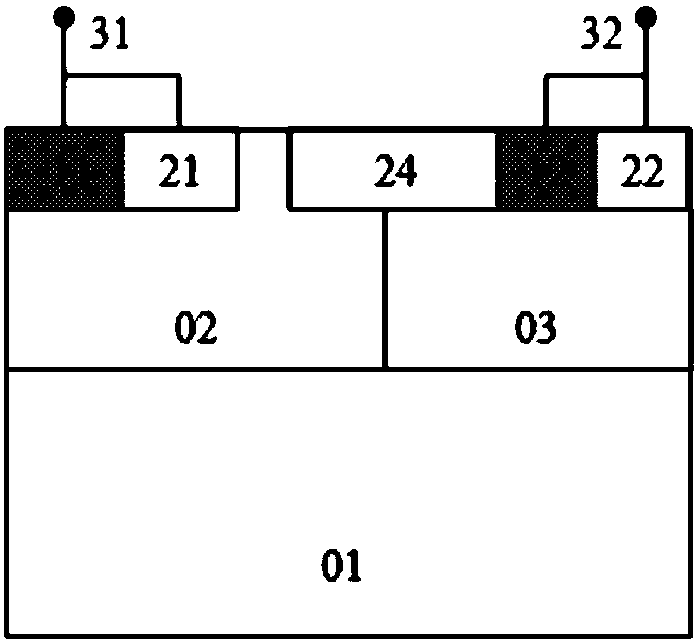
[0029] Such as figure 2 As shown, a silicon controlled rectifier for ESD protection includes: p-type substrate 01, nwell region 02 implanted on the p-type substrate, pwell region 03 tangent to the right edge of nwell region 02, and nwell region 03 The first N+ contact region 11 implanted on the surface of region 02, the first P+ region 21 tangent to the right edge of the first N+ contact region 11; the first N+ contact region 11 and the first P+ region 21 constitute an N+P+ region unit, The first N+ contact region 11 and the surface of the first P+ region 21 are short-circuited with metal to form the device anode 31; it also includes the second P+ region 22 implanted on the surface of the pwell region 03 and tangent to its right edge, and the second P+ region 22 The second N+ contact region 12 whose left edge is tangent, the adjacent second P+ region 22 and the second N+ contact region 12 form a P+N+ region unit, and the second N+ contact region 12 and the second P+ region 22...

Embodiment 2

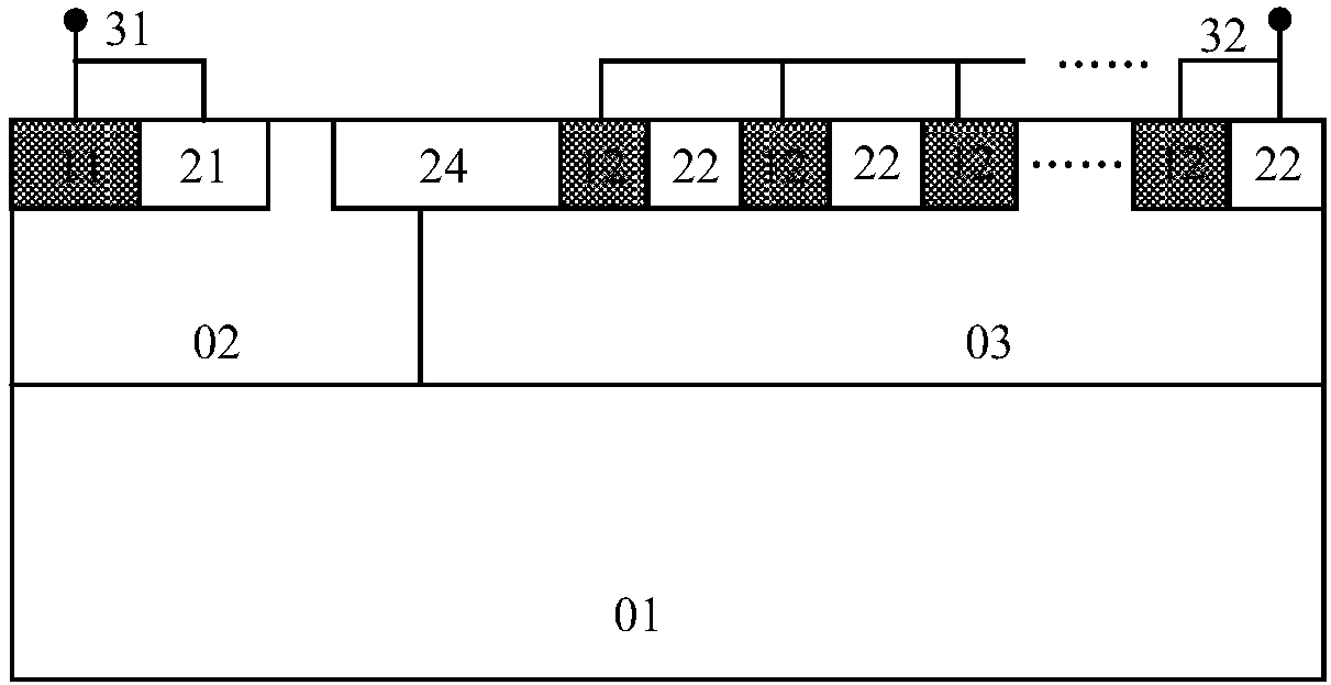
[0045] Such as image 3 As shown, the difference between this embodiment and Embodiment 1 is that: more than one P+N+ region unit is included in the pwell region 03 . The N+ area in any one of the P+N+ area units is tangent to the P+ area, and the two adjacent P+N+ area units are tangent; the second N+ contact area 12 and the rightmost The second P+ region 22 on the side is connected to form the cathode 32 of the device. By adding N+ / P+ repeating units, the vertical emission capability of the npn tube can be changed.

Embodiment 3

[0047] Such as Figure 4 As shown, the silicon controlled rectifier used for ESD protection in this embodiment includes a p-type substrate 01, an nwell region 02 formed by implantation on the p-type substrate, a pwell region 03 tangent to the right edge of the nwell region 02, The second P+ region 22 implanted on the surface of the pwell region 03 tangent to its right edge, the second N+ contact region 12 tangential to the left edge of the second P+ region 22, the adjacent second P+ region 22 and the second N+ contact The region 12 constitutes a P+N+ region unit, and the second N+ contact region 12 and the second P+ region 22 are connected to form a device cathode 32;

[0048] The first N+ contact region 11 implanted on the surface of the nwell region 02 is tangent to its left edge, the first P+ region 21 is tangent to the right edge of the first N+ contact region 11, the adjacent first N+ contact region 11 and the first The P+ area 21 constitutes an N+P+ area unit, and the n...


PUM


Abstract

The invention provides a silicon controlled rectifier (SCR) for ESD (Electro Static Discharge) protection. The SCR comprises a p-type substrate, an nwell region, a low triggering region spanning a junction of the nwell region and a pwell region, at least one N+P+ region unit set on the surface of the nwell region and at least one P+N+ region unit set on the surface of the pwell region. An N+ region and a P+ region in any N+P+ region unit are tangent. Two adjacent N+P+ region units are tangent. One side of the low triggering region and the right side of the rightmost P+ region in the at least one N+P+ region unit are tangent, or the one side of the low triggering region and the left side of the leftmost P+ region in the at least one N+P+ region unit are tangent. The low triggering region isnot tangent to the N+P+ region unit and the P+N+ region unit at the same time. The SCR cathode optimization structure for ESD provided by the invention has the obvious advantage of maximizing currentcapacity and resisting a Latch-up effect.

Description

technical field [0001] The invention belongs to the field of electronic science and technology, and is mainly used for the protection technology of Electro Static Discharge (ESD for short). Further speaking, it is a method of optimizing the cathode injection of the SCR structure, increasing the sustaining voltage by increasing the parasitic discharge path, and related device structures. Background technique [0002] ESD stands for Electrostatic Discharge, which is an ancient natural phenomenon. ESD exists in every corner of people's daily life. But it is such a common electrical phenomenon that is a fatal threat to sophisticated integrated circuits. [0003] With the improvement of integrated circuit manufacturing technology, its minimum line width has dropped to sub-micron or even nanometer level. While improving chip performance, its anti-ESD ability has also been greatly reduced, while the environment in which the device is used has not changed. , so static damage to I...

Claims


Application Information

Patent Timeline
IPC IPC(8): H01L29/87
CPCH01L29/87
Inventor 乔明齐钊肖家木王正康毛焜张波
Owner UNIV OF ELECTRONIC SCI & TECH OF CHINA
Why Eureka
Try Eureka