Anti-latch-up trigger circuit for ESD (Electronic Static Discharge)

A trigger circuit and anti-latch-up technology, which is applied to emergency protection circuit devices, circuit devices, and emergency protection circuit devices for limiting overcurrent/overvoltage, and can solve problems that cannot take into account latch-up effects and SCR structure current leakage. Maximize the discharge capacity and other issues, achieve the effect of maximizing the SCR current capacity and reducing the trigger voltage

Inactive Publication Date: 2014-09-10
UNIV OF ELECTRONICS SCI & TECH OF CHINA
View PDF4 Cites 11 Cited by
  • Summary
  • Abstract
  • Description
  • Claims
  • Application Information

AI Technical Summary

Problems solved by technology

This creates a contradiction. If you want a strong ESD current discharge capability, you cannot take into account the latch-up effect.
If you want to take into account the latch-up effect, the general approach is to increase the holding voltage of the SCR, but this will not maximize the current discharge capacity of the SCR structure

Method used


Image

  • Anti-latch-up trigger circuit for ESD (Electronic Static Discharge)
  • Anti-latch-up trigger circuit for ESD (Electronic Static Discharge)
  • Anti-latch-up trigger circuit for ESD (Electronic Static Discharge)

Examples


Embodiment 1

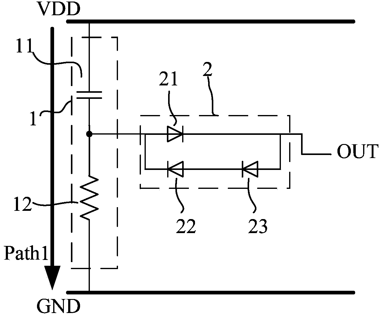
[0025] like image 3 As shown, this example includes detection circuit 1, output stage circuit 2 and SCR device connected in sequence; wherein, the detection circuit is composed of capacitor C11 and resistor R12; power supply VVD is grounded to GND through capacitor C11 and resistor R12 in turn; output stage circuit is composed of diode D21, D22, and D23; the anode of diode D21 is connected to the power supply VDD through C11, and its cathode is connected to the anode of diode D23; the cathode of diode D23 is connected to the anode of diode D22; the cathode of diode D22 is connected to the anode of diode D21; the gate of the SCR device Pole connected to the cathode of diode D21.

[0026] This example works as follows:

[0027] When the rising edge of the ESD pulse occurs on VDD, the pulse charges the upper plate of capacitor 11 . The charging current path at this time is as Figure 5 shown. When the current passes through the resistor 12, a voltage drop occurs at the upper...

Embodiment 2

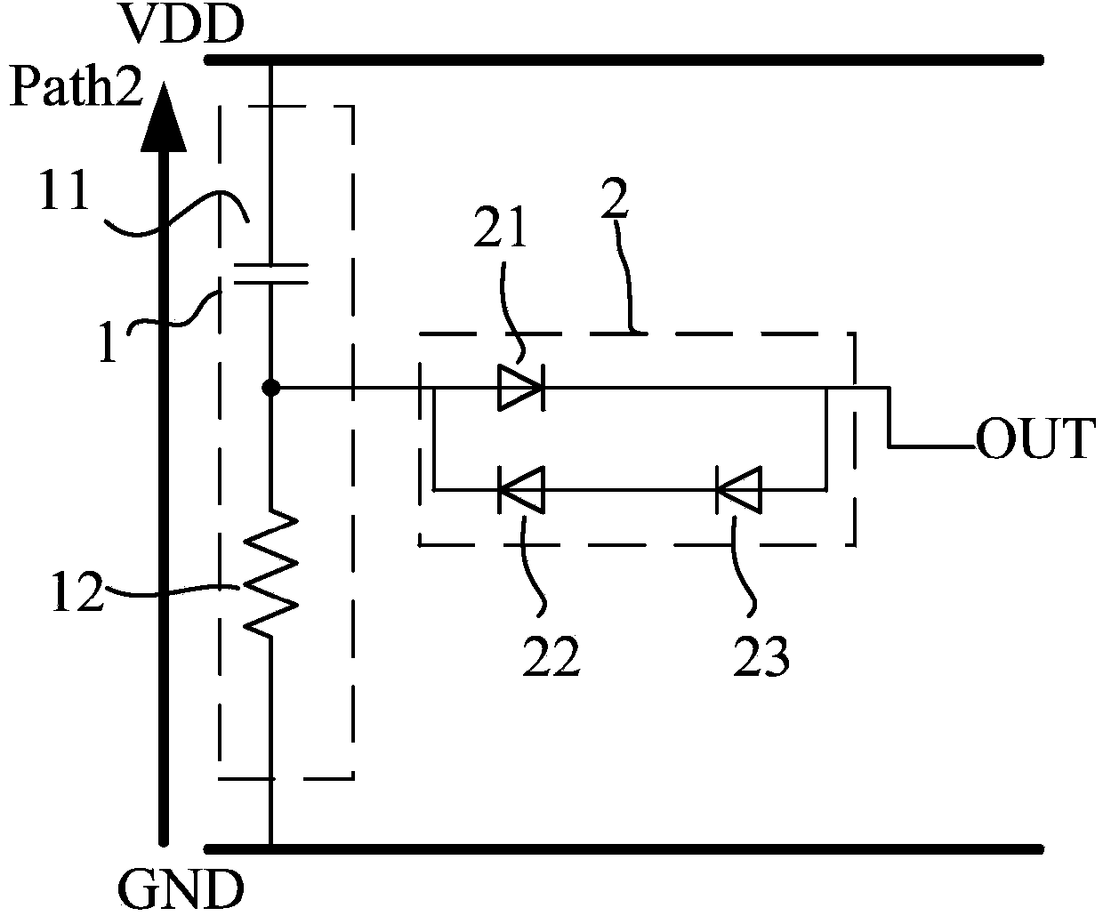
[0036] like image 3 As shown, the difference from Embodiment 1 is that a diode 13 is connected in parallel next to the resistor 12 in this example. The anode of the diode is connected to the lower plate of the capacitor 11, and its cathode is connected to GND. Other structures in the circuit remain unchanged.

[0037] Its working principle is basically the same as that of Embodiment 1, the difference is that this example uses a diode 13 to conduct the current when charging the capacitor 11 . Because the anode of the diode 13 induces a high potential when the capacitor 11 is rapidly charged to trigger the SCR. Therefore, the width-to-length ratio of the diode 13 is preferably less than 1.

[0038] Embodiment 2 sees the emulation diagram during normal power-on and the emulation diagram during ESD Figure 9 and Figure 10 .

Embodiment 3

[0040] like Figure 4 As shown, the difference from Embodiment 2 is that the diode 13 in Embodiment 2 needs to be reversely connected. That is, the cathode of the diode 13 is connected to the lower plate of the capacitor 11, the anode is connected to GND, and other structures in the circuit remain unchanged.

[0041] Its working principle is basically the same as that of Embodiment 2, except that the diode 13 is used in this example to provide the current path at the time of forward charging of the capacitor, while Embodiment 3 is just the opposite. The current path at the forward moment of the current is provided by the resistor 12, and the diode 13 only provides the capacitor discharge path. Since the circuit needs to output a higher negative potential when the capacitor is discharged, the width-to-length ratio of the diode 13 is also preferably less than 1.

[0042] Embodiment 3 sees the emulation diagram during normal power-on and the emulation diagram during ESD Figure ...


PUM


Abstract

The invention relates to the electronic circuit technology, in particular to an anti-latch-up trigger circuit for ESD. The circuit comprises a detection circuit 1, an output stage circuit 2 and an SCR (Silicon Controlled Rectifier) which are connected in sequence; the detection circuit is composed of a capacitor C11 and a resistor R12, and a power supply VVD is connected with the ground GND after sequentially passing through the capacitor C11 and the resistor R12; the output stage circuit is composed of a diode D21, a diode D22, a diode D23, the positive electrode of the diode D21 is connected with the power supply VDD after passing through the C11, the negative electrode of the diode D21 is connected with the positive electrode of the diode D23, the negative electrode of the diode D23 is connected with the positive electrode of the diode D22, and the negative electrode of the diode D22 is connected with the positive electrode of the diode D21; the gate pole of the SCR is connected with the negative electrode of the diode D21. The anti-latch-up trigger circuit for ESD has the advantages of having significant effects on maximizing the current capability of the SCR and reducing the trigger voltage of the SCR and being capable of capturing the falling edge of the ESD pulse and outputting negative voltage to turn off the SCR structure. The anti-latch-up trigger circuit is particularly suitable for ESD.

Description

technical field [0001] The invention relates to electronic circuit technology, mainly used for electrostatic discharge (Electro Static Discharge, referred to as ESD for short) protection technology, specifically a kind of can identify the falling edge of ESD pulse and output closing signal to turn off the clamping device , Prevent latch-up (Latch-up) trigger circuit. Background technique [0002] ESD stands for Electrostatic Discharge, which is a common phenomenon in nature. ESD exists in every corner of people's daily life. But it is such a common electrical phenomenon that is a fatal threat to sophisticated integrated circuits. [0003] With the improvement of integrated circuit manufacturing technology, its minimum line width has dropped to submicron or even nanometer level. While improving chip performance, its ability to resist ESD is also greatly reduced, so electrostatic damage is more serious. The contradiction between process development and chip ESD resistance h...

Claims


Application Information

Patent Timeline
Patent Type & Authority Applications(China)
IPC IPC(8): H02H9/04
Inventor 乔明齐钊马金荣薛腾飞张波
Owner UNIV OF ELECTRONICS SCI & TECH OF CHINA
Why Eureka
Try Eureka