Latch-free SCR for ESD protection

A latch and substrate technology, applied in the field of latch-free SCR, can solve the problems of reduced secondary breakdown current, increased power consumption, logic errors, etc., to achieve lower trigger voltage, better ESD protection, and anti-Latch-up Effect

Active Publication Date: 2017-02-22
UNIV OF ELECTRONICS SCI & TECH OF CHINA
View PDF4 Cites 3 Cited by
  • Summary
  • Abstract
  • Description
  • Claims
  • Application Information

AI Technical Summary

Problems solved by technology

If LVTSCR is used to protect the signal port, when the circuit is powered on, the transient noise signal or ESD signal will cause the normal signal to be clamped, which will cause logic errors and cause immeasurable consequences
Although increasing the maintenance voltage of LVTSCR can avoid Latch-up, but due to the increase of its power consumption, the ESD capability will decrease, and the secondary breakdown current It2 will decrease

Method used


Image

  • Latch-free SCR for ESD protection
  • Latch-free SCR for ESD protection
  • Latch-free SCR for ESD protection

Examples


Embodiment 1

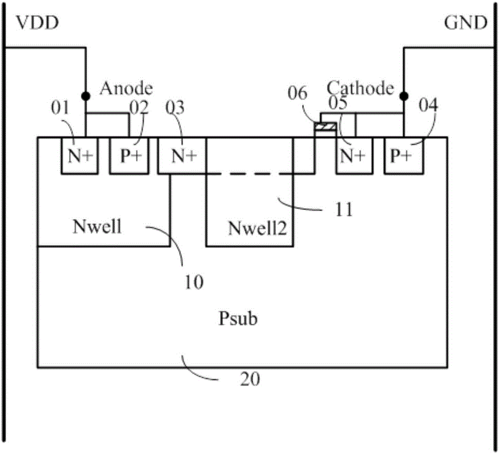
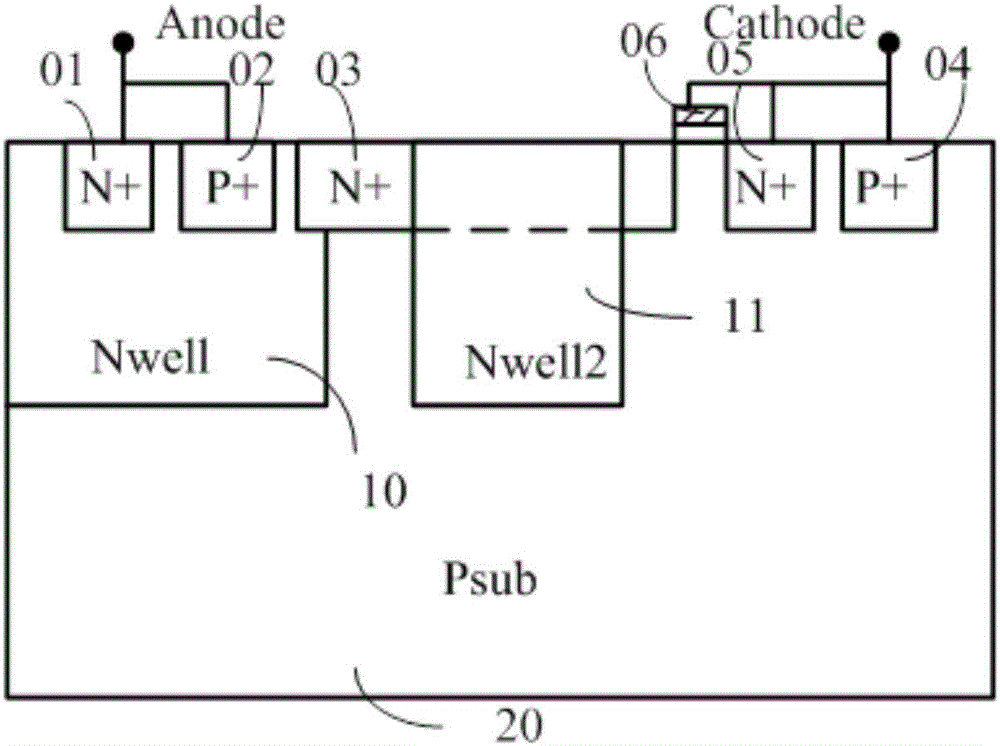
[0020] Such as figure 2 As shown, the latch-free SCR for ESD protection in this example includes a P-type substrate 20; the upper layer of the P-type substrate has a first N well 10, a surface N+ layer 03, a second N well 11, cathode contact N+ region 05, and cathode contact P+ region 04; the surface N+ layer 03 is partly located in the first N well 10, the upper layer of the second N well 11 overlaps with the surface N+ layer 03, and the surface N+ layer The horizontal width of 03 is greater than the horizontal width of the second N well 11; the upper layer of the first N well 10 has an anode contact N+ region 01 and an anode contact P+ region 02 that are independent of each other, and the anode contact P+ region 02 is located near the surface N+ layer 03 one side; the upper surface of the P-type substrate 20 between the surface N+ layer 03 and the cathode contact N+ region 05 has a gate 06; the anode contact N+ region 01 and the anode contact P+ region 02 are connected with...

Embodiment 2

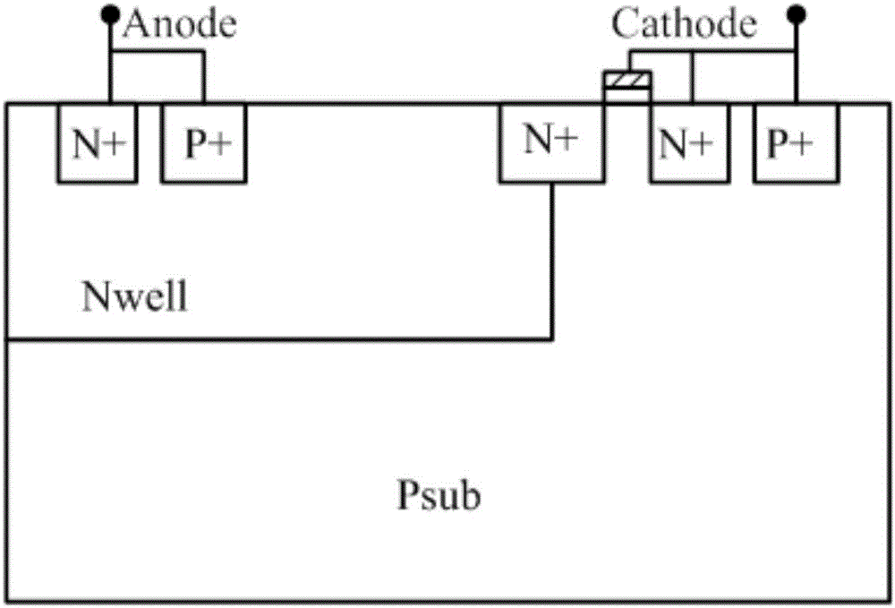
[0025] Such as Figure 4 As shown, the difference from Embodiment 1 is that the second N well 11 in Embodiment 1 needs to be removed and other structures remain unchanged.

[0026] Its working principle is basically the same as that of Embodiment 1, except that Embodiment 2 additionally uses the conduction of the second parasitic NPN transistor (by N+ / PSub+P+ / Nwell) to control the sustain voltage. The rest of the principles are basically the same.

Embodiment 3

[0028] Such as Figure 5 As shown, the difference from Embodiment 2 is that the second N well 11 needs to be removed and replaced with the Ptop layer 08, and other structures remain unchanged.

[0029] Its working principle is basically the same as that of Embodiment 2.


PUM


Abstract

The invention, which belongs to the field of the electronic science and technology, especially to the field of the electro static discharge (ESD) technology, particularly relates to a latch-free silicon controlled rectifier (SCR) for ESD protection. According to the SCR device provided by the invention, surface N+ injection is carried out, thereby reducing a current amplification factor of a parasitic PNP device and thus improving the maintaining voltage of the device to prevent a latch-up effect. Besides, on the basis of shunting of anode currents by a plurality of parasitic PNP tubes, heat distribution of the anode is optimized, thereby improving the secondary breakdown current of the device.

Description

technical field [0001] The invention belongs to the field of electronic science and technology, and is mainly used for electrostatic discharge (Electro Static Discharge, referred to as ESD) protection technology, and specifically relates to a latch-free SCR (Silicon Controlled Rectifier, silicon controlled rectifier) ​​for ESD protection . Background technique [0002] ESD stands for Electrostatic Discharge, which is a common phenomenon in nature. ESD exists in every corner of people's daily life. But it is such a common electrical phenomenon that is a fatal threat to sophisticated integrated circuits. [0003] With the improvement of integrated circuit manufacturing technology, its minimum line width has dropped to submicron or even nanometer level. While improving chip performance, its ability to resist ESD is also greatly reduced, so electrostatic damage is more serious. The contradiction between process development and chip ESD resistance has become a problem that IC ...

Claims


Application Information

Patent Timeline
Patent Type & Authority Applications(China)
IPC IPC(8): H01L29/06H01L29/861
CPCH01L29/0684H01L29/8611
Inventor 乔明齐钊杨文张波
Owner UNIV OF ELECTRONICS SCI & TECH OF CHINA
Why Eureka
Try Eureka