Electrostatic Discharge Protection Device Comprising a Silicon Controlled Rectifier

a technology of electronic discharge protection and rectifier, which is applied in the direction of semiconductor devices, semiconductor/solid-state device details, diodes, etc., can solve the problems of latching during testing or thereafter, early trigger of mos devices is unwanted, and trigger voltage too high to be usable in many designs, etc., to achieve higher resistivity, reduce trigger voltage, and reduce the effect of trigger voltag

Active Publication Date: 2017-01-12
NXP BV
View PDF4 Cites 11 Cited by
  • Summary
  • Abstract
  • Description
  • Claims
  • Application Information

AI Technical Summary

Benefits of technology

[0013]a blocking region having a higher resistivity than the region having the second conductivity type, wherein the blocking region is located between the contact region of the first conductivity type and the contact region of the second conductivity type in the region having the second conductivity type, for reducing a trigger voltage of the silicon controlled rectifier.
[0014]The provision of the blocking region having a higher resistivity than the region having the second conductivity type may reduce the trigger voltage of the silicon controlled rectifier. In some examples the reduced trigger voltage may allow the silicon controlled rectifier to trigger before triggering of a device (e.g. an output stage MOS) that the ESD protection device is intended to protect. This may avoid failure of the protected device during an ESD event. Accordingly, the reduced trigger voltage that may be provided by the blocking region may allow the device to be used in a wider range of applications (e.g. for applications that require ESD protection for smaller output stage MOS devices).
[0015]The device may include a further region having the first conductivity type located adjacent the region having the second conductivity type in the semiconductor substrate. A contact region of the first conductivity type and a contact region of the second conductivity type may be located in the further region having the first conductivity type. This arrangement may allow the failure current of the device (It2) to be increased.
[0016]The device may be connected to provide ESD protection that, during an ESD event, may shunt an ESD current from a first node (which may be a power supply rail or I / O pad of the device) to a second node (which may be a ground rail of the device).

Problems solved by technology

A challenge related to pad-based ESD design is that the ESD protection device often has a higher trigger voltage than the trigger voltage of a driver MOS device to be protected.
Triggering of the MOS devices may thus occur earlier than triggering of the ESD device when the gate voltage of the driver MOS is uncontrolled and unknown during an ESD event.
An early trigger of the MOS device is unwanted because it may lead to immediate failure.
However, traditional SCR designs typically have a trigger voltage that is too high to be usable in many designs.
Furthermore, an SCR typically has low holding voltage (i.e. the voltage at which the current shunting mode operates, after triggering the SCR), which can lead to latch-up during testing or thereafter when an ESD event occurs.
Latch-up generally leads to device failure.

Method used


Image

  • Electrostatic Discharge Protection Device Comprising a Silicon Controlled Rectifier
  • Electrostatic Discharge Protection Device Comprising a Silicon Controlled Rectifier
  • Electrostatic Discharge Protection Device Comprising a Silicon Controlled Rectifier

Examples


Embodiment Construction

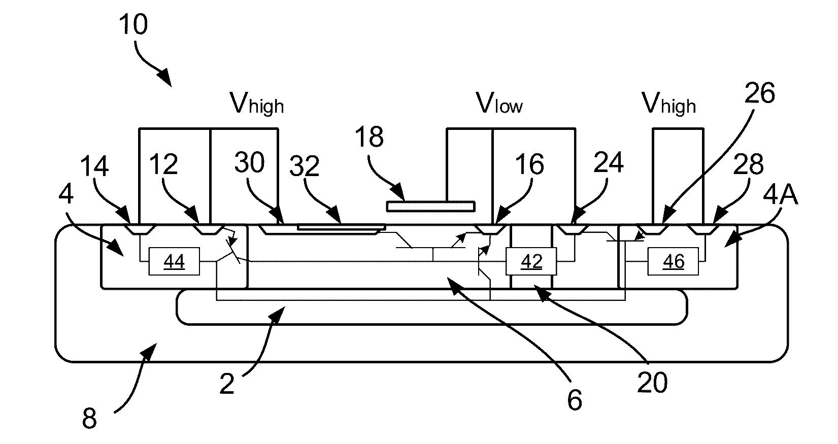
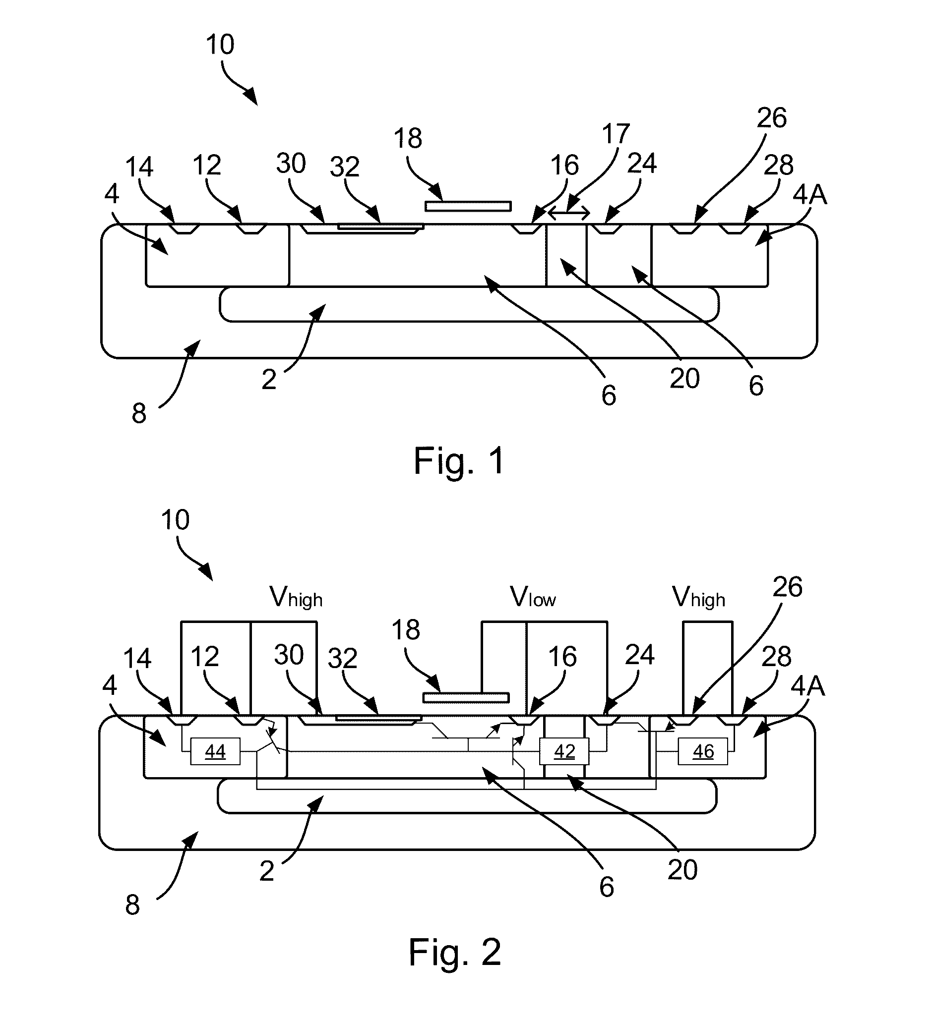
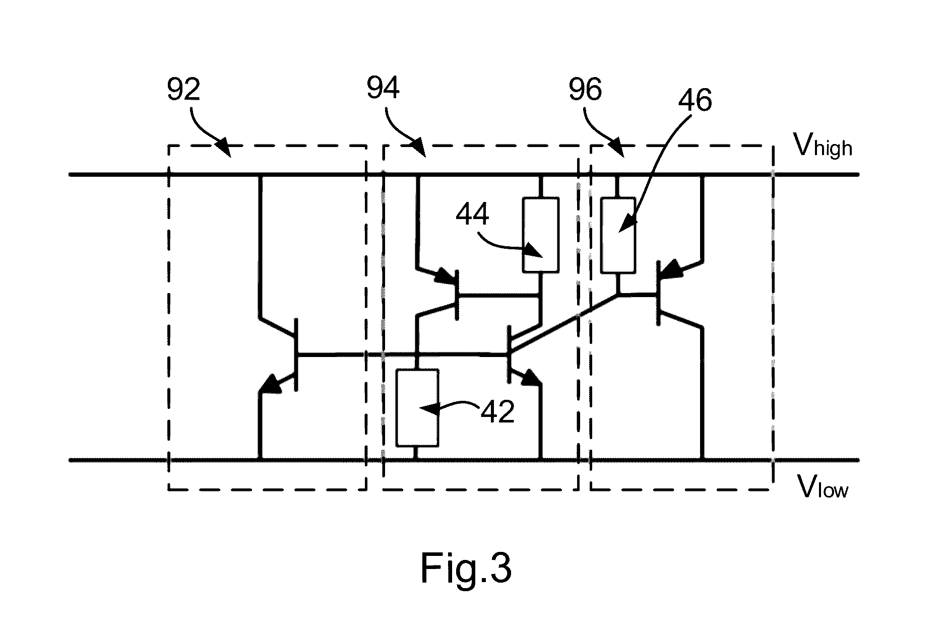
[0043]Embodiments of the present disclosure are described in the following with reference to the accompanying drawings.

[0044]Embodiments of this disclosure may provide an electrostatic discharge (ESD) protection device that comprises a silicon controlled rectifier (SCR). The device can be provided in a semiconductor substrate, such as a silicon substrate.

[0045]The following embodiments are described in the context of devices for which the first conductivity type is n-type and the second conductivity type is p-type. Nevertheless, as noted above, it is envisaged that the first conductivity type may be p-type and the second conductivity type may be n-type.

[0046]The device includes region having a first conductivity type (in the examples described below, a first n-type region) located in the substrate. The device includes region having a second conductivity type (in the examples described below, a first p-type region), which is also located in the substrate. The region having the second...


PUM


Abstract

An electrostatic discharge protection device including a silicon controlled rectifier. In one example, the silicon controlled rectifier includes a first n-type region located in a semiconductor substrate. The silicon controlled rectifier also includes a first p-type region located adjacent the first n-type region in the semiconductor substrate. The silicon controlled rectifier further includes an n-type contact region and a p-type contact region located in the first n-type region. The silicon controlled rectifier also includes an n-type contact region and a p-type contact region located in the first p-type region. The silicon controlled rectifier further includes a blocking region having a higher resistivity than the first p-type region. The blocking region is located between the n-type contact region and the p-type contact region in the first p-type region for reducing a trigger voltage of the silicon controlled rectifier.

Description

FIELD OF THE INVENTION[0001]This invention relates to an electrostatic discharge protection device comprising a silicon controlled rectifier.BACKGROUND OF THE INVENTION[0002]Integrated circuits generally include an electrostatic discharge (ESD) device for shunting currents which occur during the manufacturing process (e.g. due to discharging of a charged human body (‘human body model’, or ‘HBM’)). In pad-based ESD designs, in particular, the ESD protection is usually placed locally, and is connected to the drains of an output stage MOS. During an ESD event, current shunting occurs after a trigger voltage across the ESD device has been reached. When the ESD device triggers, its voltage drops to a holding voltage. The trigger voltage of the ESD device should therefore be above a maximum operating voltage of the product.[0003]A challenge related to pad-based ESD design is that the ESD protection device often has a higher trigger voltage than the trigger voltage of a driver MOS device t...

Claims


Application Information

Patent Timeline
Patent Type & Authority Applications(United States)
IPC IPC(8): H01L27/02H01L23/528H01L29/06
CPCH01L27/0262H01L23/5286H01L29/0684H01L23/60H01L27/02H01L29/87H01L29/0692
Inventor QUAX, GUIDO WOUTER WILLEMLAI, DA-WEI
Owner NXP BV
Why Eureka
Try Eureka