Bidirectional ESD protection anti-latch-up device of holosymmetric dual-grid-control-diode triggering SCR structure

A gated diode and ESD protection technology, applied in diodes, electro-solid devices, semiconductor devices, etc., can solve the problems of high trigger voltage and low sustain voltage, and achieve the effect of reducing the trigger voltage and improving the turn-on speed.

Active Publication Date: 2018-02-02
JIANGNAN UNIV
View PDF6 Cites 12 Cited by
  • Summary
  • Abstract
  • Description
  • Claims
  • Application Information

AI Technical Summary

Problems solved by technology

[0004] Aiming at the common problems of high trigger voltage and low maintenance voltage in ESD protection devices with SCR structure, the present invention designs a bidirectional ESD protection anti-latch-up device with fully symmetrical double gate control diode triggering SCR structure, making full use of the resistance Capacitive coupling circuit has the advantages of low trigger voltage and fast turn-on speed, combined with the advantages of strong ESD robustness of SCR structure, and effectively shunts ESD pulses by forming multiple current discharge paths, so that the design device can be formed under ESD stress. RC-coupled auxiliary trigger path composed of parasitic P-well resistance, gated diode and high sustain voltage path composed of longitudinal bias NPN and parasitic well resistance

Method used


Image

  • Bidirectional ESD protection anti-latch-up device of holosymmetric dual-grid-control-diode triggering SCR structure
  • Bidirectional ESD protection anti-latch-up device of holosymmetric dual-grid-control-diode triggering SCR structure
  • Bidirectional ESD protection anti-latch-up device of holosymmetric dual-grid-control-diode triggering SCR structure

Examples


Embodiment Construction

[0027] Below in conjunction with accompanying drawing and specific embodiment the present invention will be described in further detail:

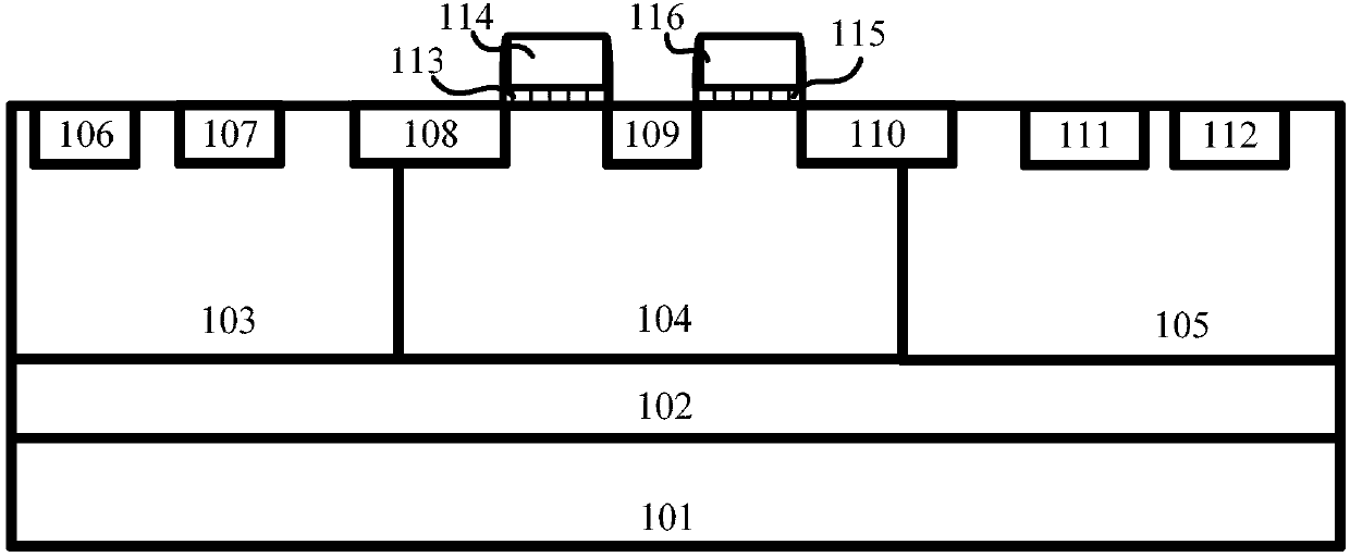
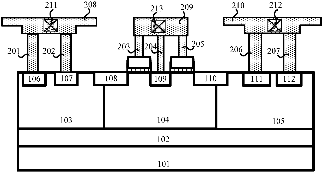
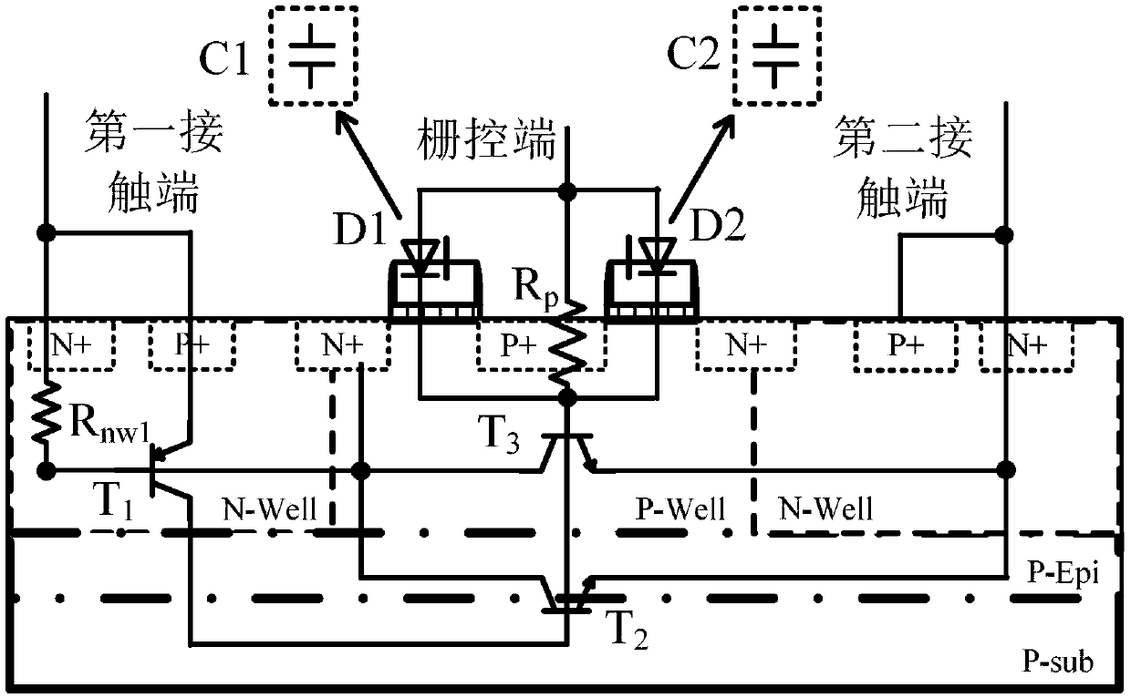
[0028] The example of the present invention designs a bidirectional ESD protection anti-latch-up device with a fully symmetrical double gate-controlled diode triggering SCR structure, making full use of the advantages of low trigger voltage and fast turn-on speed of the resistance-capacitance coupling circuit, combined with the strong ESD robustness of the SCR structure advantages, and by forming multiple current discharge paths to effectively shunt ESD pulses, the designed device can form a resistance-capacitance coupling auxiliary trigger path composed of parasitic P-well resistance and a gate-controlled diode under the action of ESD stress, and a longitudinal bias The high sustain voltage path composed of NPN and parasitic well resistance, also has a fully symmetrical layout structure composed of the first N well, P well and second N well...


PUM


Abstract

The invention discloses a bidirectional ESD protection anti-latch-up device of a holosymmetric dual-grid-control-diode triggering SCR structure, and the device can be used for improving the capabilityof an IC chip in resisting ESD. The device mainly consists of a P substrate, a P epitaxial part, a first N well, a P well, a second N well, a first N+ injection region, a first P+ injection region, asecond N+ injection region, a second P+ injection region, a third N+ injection region, a third P+ injection region, a fourth N+ injection region, a first polysilicon gate, a first thin gate oxide layer covering the first polysilicon gate, a second polysilicon gate, and a second thin gate oxide layer covering the second polysilicon gate. The device has a resistance-capacitance coupling auxiliary triggering path under the action of ESD stress, does not need an additional layout area, also can make the most of the advantages of low triggering voltage of a resistance-capacitance coupling circuitand the short start time, and shortens the voltage hysteresis amplitude of the device. In addition, the device also employs the conduction characteristics of the gate control diodes, improves the potential of a parasitic well resistor of the N well, and speeds up the starting of a current releasing path of the SCR structure. Moreover, the device has two ESD current releasing paths and a holosymmetric structure, facilitates the improvement of the ESD robustness of the device, and can achieve the bidirectional protection of ESD.

Description

technical field [0001] The invention belongs to the field of electrostatic discharge protection of integrated circuits and relates to an ESD protection device, in particular to a bidirectional ESD protection and anti-latch-up device with a fully symmetrical double gate control diode triggering SCR structure, which can be used to improve the reliability of ESD protection of integrated circuits . Background technique [0002] With the rapid development of integration technology, people's demand for multi-functionality and portability of electronic products is increasing, and the integration level of integrated circuit (IC) chips is increasing day by day. On the one hand: the rapid progress of integrated technology has greatly improved the performance and energy efficiency of circuit systems on the one hand, and on the other hand, the reliability of IC chips is facing increasingly severe challenges. According to investigations: about 30%-40% of IC chip failures are caused by e...

Claims


Application Information

Patent Timeline
Patent Type & Authority Applications(China)
IPC IPC(8): H01L27/02
CPCH01L27/0255H01L27/0288H01L27/0296
Inventor 顾晓峰马艺珂梁海莲丁盛
Owner JIANGNAN UNIV
Why Eureka
Try Eureka