Silicon controlled device with double-conduction path

A thyristor, double conduction technology, applied in semiconductor devices, electric solid devices, circuits, etc., can solve the problems of uneven conduction between the surface of the ESD device and the inside of the device, high trigger voltage of the thyristor, and ineffective protection. , to achieve the effect of good device robustness, high ESD efficiency and uniform current

Inactive Publication Date: 2011-08-10
ZHEJIANG UNIV
View PDF4 Cites 11 Cited by
  • Summary
  • Abstract
  • Description
  • Claims
  • Application Information

AI Technical Summary

Problems solved by technology

Therefore, the trigger voltage of the thyristor is relatively high, and it cannot effectively protect the working voltage of 5V and below.
At the same time, according to the principle that electrons always choose the shortest path, the electronic current in the ESD device will choose the shortest conduction path. When the device discharges the ESD current, the current density on the surface of the device is always the largest, so there is an ESD device on the surface and inside the device. The problem of uneven conduction

Method used


Image

  • Silicon controlled device with double-conduction path
  • Silicon controlled device with double-conduction path
  • Silicon controlled device with double-conduction path

Examples


Embodiment Construction

[0019] The present invention will be described in detail below in conjunction with the embodiments and accompanying drawings, but the present invention is not limited thereto.

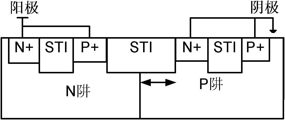
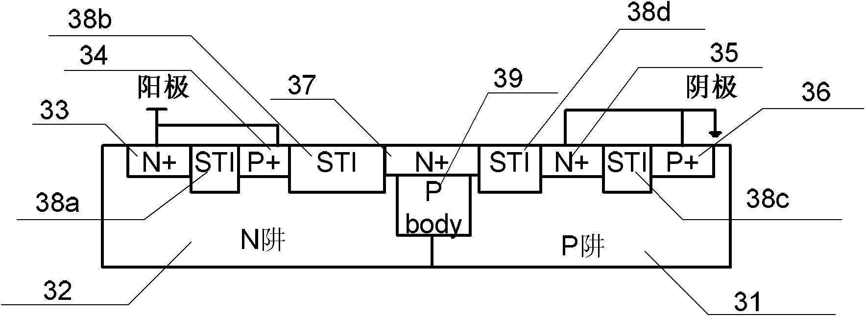
[0020] Such as image 3 and Figure 4 As shown, a thyristor device with dual conduction paths includes adjacent N well 32 and P well 31, wherein the direction from N well 32 to P well 31, in N well 32 and P well 31 A first N+ implantation region 33, a first shallow trench isolation 38a, a first P+ implantation region 34, a second shallow trench isolation 38b, a third N+ implantation region 37, a fourth shallow trench isolation 38d, a second N+ Implantation region 35, the third shallow moat isolation 38c and the second P+ implantation region 36; the third N+ implantation region 37 is arranged at the junction of N well 32 and P well 31, and the two ends of the third N+ implantation region 37 are set across the N On the well 32 and the P well 31; the first N+ implantation region 33 and the first P+ impl...


PUM


Abstract

The invention discloses a silicon controlled device with a double-conduction path. The silicon controlled device comprises a P well and an N well, wherein an N+ injection region and a Pbody region are spanned between the P well and the N well. The N+ injection region spanned between the P well and the N well is used for realizing reduction of the silicon controlled trigger voltage; and the Pbody region at a junction between the N well and the P well is used for realizing separation between a silicon controlled surface current path and a silicon controlled internal current path. Compared with the common SCR (silicon controlled rectifier) structure which has the defects that more currents are concentrated on the surface of the device, and the conduction uniformity is bad, the silicon controlled device with the double-conduction path has simple structure, good conduction uniformity, high ESD (electro-static discharge) efficiency and good robustness and is suitable for electrostatic discharge protection of high voltage circuits and power circuits.

Description

technical field [0001] The invention belongs to the field of electrostatic protection of integrated circuits, and in particular relates to a thyristor device with double conduction paths. Background technique [0002] The phenomenon of electrostatic discharge (ESD) in nature poses a serious threat to the reliability of integrated circuits. In the industry, 30% of the failures of integrated circuit products are caused by electrostatic discharge, and the increasingly smaller process size and thinner gate oxide thickness greatly increase the probability of integrated circuit damage by electrostatic discharge. Therefore, improving the reliability of integrated circuit electrostatic discharge protection has a non-negligible effect on improving the yield of products. [0003] The modes of electrostatic discharge phenomena are usually divided into four types: HBM (Human Body Model), MM (Machine Discharge Model), CDM (Component Charge Discharge Model) and Field Induction Model (FIM...

Claims


Application Information

Patent Timeline
Patent Type & Authority Applications(China)
IPC IPC(8): H01L29/747H01L29/06H01L27/02
CPCH01L29/87
Inventor 苗萌董树荣李明亮吴健韩雁马飞宋波郑剑锋
Owner ZHEJIANG UNIV
Why Eureka
Try Eureka