Manufacturing method for ESD gate grounding NMOS transistor

A manufacturing method and transistor technology, applied in semiconductor/solid-state device manufacturing, electrical components, circuits, etc., can solve the problems of wasting the area occupied by devices, and achieve the effects of saving area, saving cost, and simplifying the process

Inactive Publication Date: 2009-06-10
SHANGHAI HUA HONG NEC ELECTRONICS
View PDF0 Cites 11 Cited by
  • Summary
  • Abstract
  • Description
  • Claims
  • Application Information

AI Technical Summary

Problems solved by technology

Since the source and drain are heavily doped regions, the sheet resistance is very small, so the manufacturing of NMOS transistors according to the above conventional method needs to leave a large gap to meet the series resistance requirements, so it is a waste of the area occupied by the device.

Method used


Image

  • Manufacturing method for ESD gate grounding NMOS transistor
  • Manufacturing method for ESD gate grounding NMOS transistor
  • Manufacturing method for ESD gate grounding NMOS transistor

Examples


Embodiment Construction

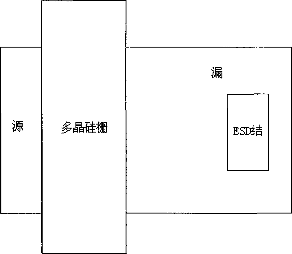
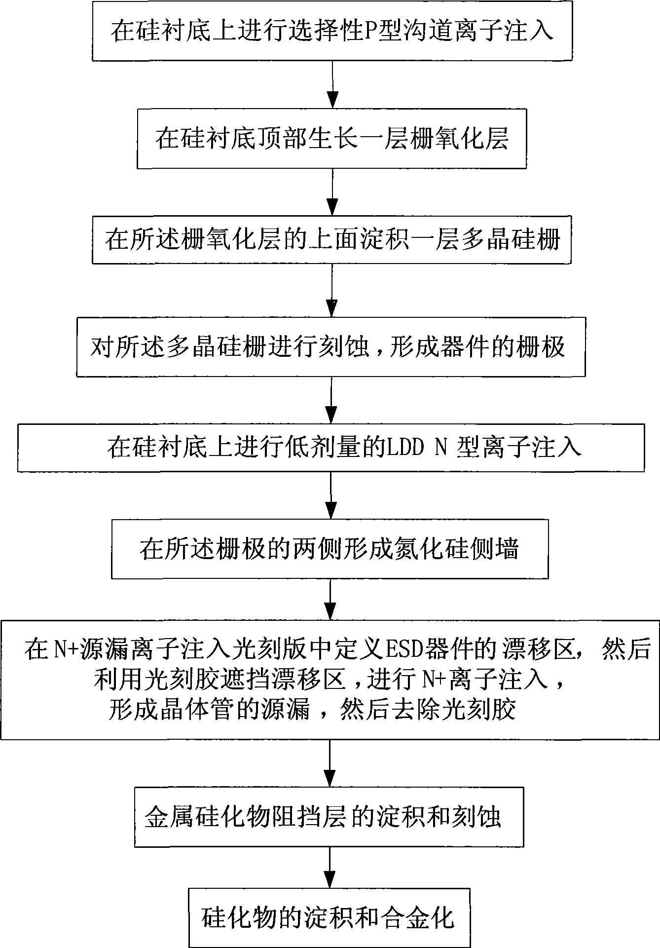
[0016] In one embodiment, such as image 3 As shown, the ESD gate grounding NMOS transistor manufacturing method of the present invention comprises the following steps:

[0017] In the first step, selective P-type channel ion implantation is performed on the silicon substrate.

[0018] In the second step, a gate oxide layer is grown on the top of the silicon substrate, and then a polysilicon gate is deposited on the gate oxide layer.

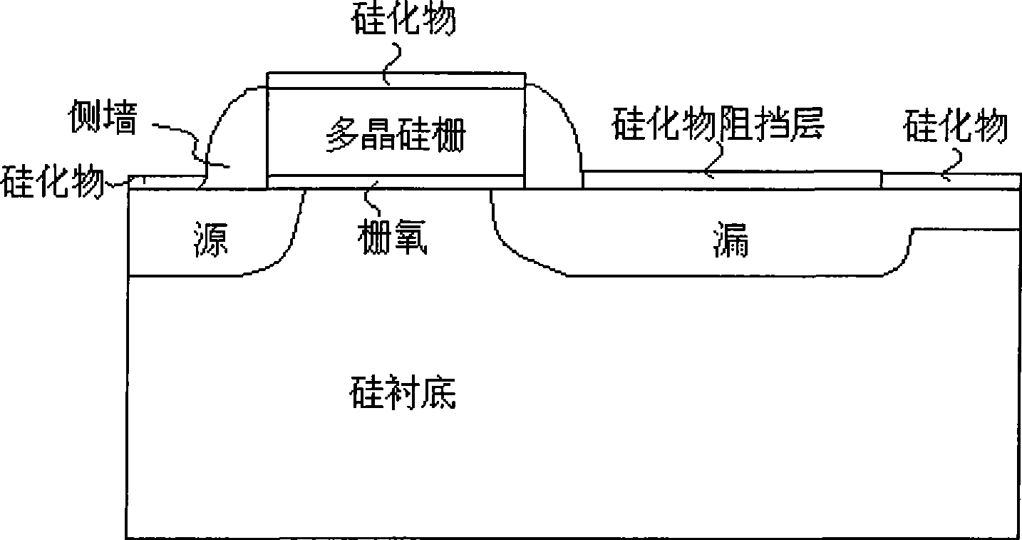
[0019] The third step is to use known photolithography technology to etch the polysilicon gate to form the gate of the device. The cross-sectional structure at this time is as follows Figure 4a shown.

[0020] The fourth step is to perform selective low-dose LDD (Lightly Doped Drain, lightly doped drain) N-type ion implantation on the silicon substrate to form a lightly doped LDD region, where the implanted ion dose ranges from E13 to E14cm -2 .

[0021] In the fifth step, silicon nitride sidewalls are formed on both sides of the gate.

...


PUM


Abstract

The invention discloses a method for manufacturing an ESD gate grounded NMOS transistor. Through photoetching, the drain end and the edge of the grid electrode of the ESD transistor are in certain distance; a region (a drift region) between the drain end and the grid electrode is only provided with a lightly-doped source drain (LDD) region and no high-dosage drain adulteration; as square resistance of the LDD region is much larger relative to the high doped drain end, the method can ensure that larger series resistance is obtained under the condition of shorter length of the drift region without increasing area occupied by the transistor, thereby saving the area of the transistor; moreover, as the breakdown voltage of an LDD junction is lower than the drain end, the transistor decides the trigger voltage through the LDD junction, well achieves the aim of reducing the trigger voltage, does not need any extra ESD photoetching and ESD ion injection, thereby simplifying a process and saving cost.

Description

technical field [0001] The invention relates to the field of manufacturing semiconductor devices, in particular to a method for manufacturing an ESD gate-grounded NMOS transistor. Background technique [0002] Electrostatic protection (ESD) gate-grounded NMOS (GGNMOS) breaks down through the junction of the drain to turn on the drain / channel / source parasitic bipolar transistor to achieve the effect of discharging static electricity. In order to have a better protection effect from ESD, the trigger voltage of the drain needs to be appropriately reduced, and in addition, a large series resistance is required at the drain terminal to adjust the thermal breakdown voltage of the ESD transistor. Conventional ESD gate-grounded NMOS transistors generally use a self-aligned source-drain process, that is, first use the gate and sidewalls to perform source-drain ion implantation, and then in order to achieve a large drain terminal series resistance, it is necessary to insert Leave a l...

Claims


Application Information

Patent Timeline
Patent Type & Authority Applications(China)
IPC IPC(8): H01L21/336H01L21/266
Inventor 钱文生
Owner SHANGHAI HUA HONG NEC ELECTRONICS
Why Eureka
Try Eureka