An anti-latch trigger circuit for esd
A trigger circuit and anti-latch-up technology, which is applied in the direction of emergency protection circuit devices, circuit devices, emergency protection circuit devices, etc. for limiting overcurrent/overvoltage, can solve the problem of not being able to maximize the current discharge capacity of the SCR structure, and not being able to Taking into account issues such as latch-up effects to maximize the SCR current capability and reduce the trigger voltage
- Summary
- Abstract
- Description
- Claims
- Application Information
AI Technical Summary
Problems solved by technology
Method used
Image
Examples
Embodiment 1
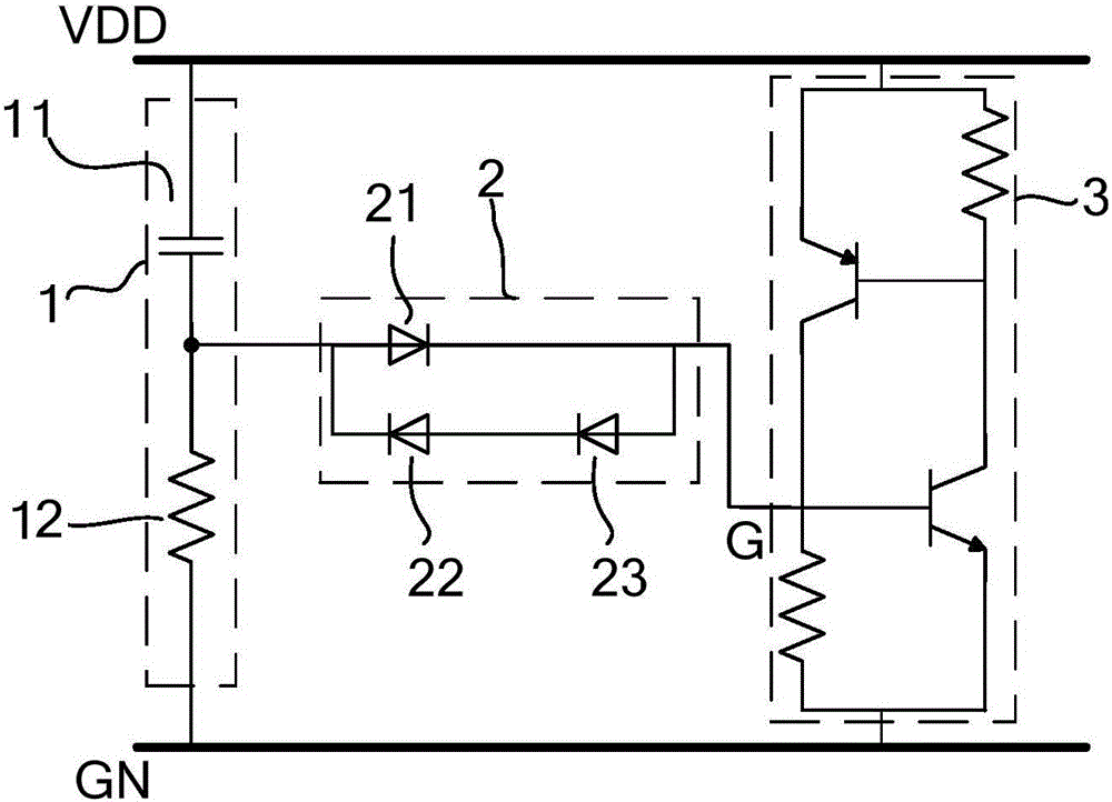
[0025] Such as figure 2 As shown, this example includes detection circuit 1, output stage circuit 2 and SCR device connected in sequence; wherein, the detection circuit is composed of capacitor C11 and resistor R12; the power supply VDD is grounded to GND through capacitor C11 and resistor R12 in turn; the output stage circuit is composed of diode D21, D22, and D23; the anode of diode D21 is connected to the power supply VDD through C11, and its cathode is connected to the anode of diode D23; the cathode of diode D23 is connected to the anode of diode D22; the cathode of diode D22 is connected to the anode of diode D21; the gate of the SCR device Pole connected to the cathode of diode D21.
[0026] This example works as follows:
[0027] When the rising edge of the ESD pulse occurs on VDD, the pulse charges the upper plate of capacitor 11 . The charging current path at this time is as Figure 5 shown. When the current passes through the resistor 12, a voltage drop occurs ...
Embodiment 2
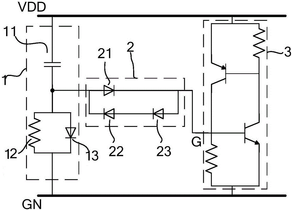
[0036] Such as image 3 As shown, the difference from Embodiment 1 is that a diode 13 is connected in parallel next to the resistor 12 in this example. The anode of the diode is connected to the lower plate of the capacitor 11, and its cathode is connected to GND. Other structures in the circuit remain unchanged.
[0037] Its working principle is basically the same as that of Embodiment 1, the difference is that this example uses a diode 13 to conduct the current when charging the capacitor 11 . Because the anode of the diode 13 induces a high potential when the capacitor 11 is rapidly charged to trigger the SCR. Therefore, the width-to-length ratio of the diode 13 is preferably less than 1.
[0038] Embodiment 2 sees the emulation diagram during normal power-on and the emulation diagram during ESD Figure 9 and Figure 10 .
Embodiment 3
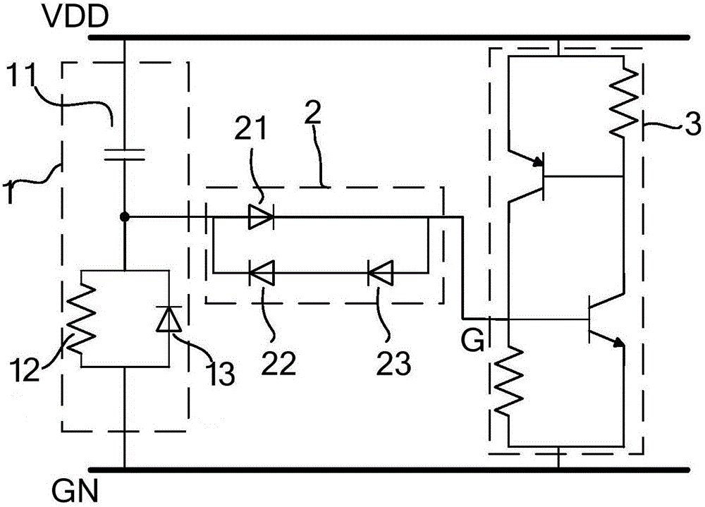
[0040] Such as Figure 4 As shown, the difference from Embodiment 2 is that the diode 13 in Embodiment 2 needs to be reversely connected. That is, the cathode of the diode 13 is connected to the lower plate of the capacitor 11, the anode is connected to GND, and other structures in the circuit remain unchanged.
[0041] Its working principle is basically the same as that of Embodiment 2, except that the diode 13 is used in this example to provide the current path at the time of forward charging of the capacitor, while Embodiment 3 is just the opposite. The current path at the forward moment of the current is provided by the resistor 12, and the diode 13 only provides the capacitor discharge path. Since the circuit needs to output a higher negative potential when the capacitor is discharged, the width-to-length ratio of the diode 13 is also preferably less than 1.
[0042] Embodiment 3 sees the emulation diagram during normal power-on and the emulation diagram during ESD Figu...
PUM
 Abstract
Description
Claims
Application Information


