Process for manufacturing wiring substrate
A wiring substrate and manufacturing method technology, which is applied in the fields of printed circuit manufacturing, semiconductor/solid-state device manufacturing, chemical/electrolytic method to remove conductive materials, etc., can solve the problem of insufficient electrical connection between connection pads and solder balls, and difficulty in reliable fixing Problems such as electrical connection of electrode terminals of electronic components
- Summary
- Abstract
- Description
- Claims
- Application Information
AI Technical Summary
Problems solved by technology
Method used
Image

Examples
Embodiment 1)
[0181]
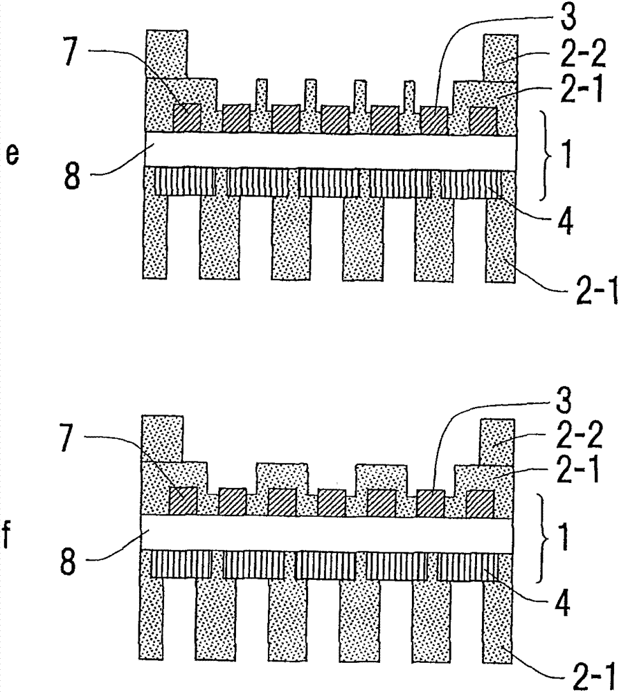
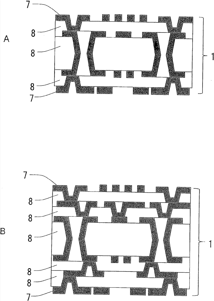
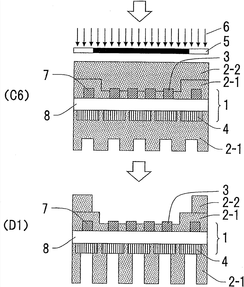
[0182] The circuit board 1 (170 mm x 200 mm in area, 15 µm in conductor thickness, and 0.4 mm in substrate thickness) was fabricated using the semi-additive method. Conductor wiring with a line width of 25 µm and a pitch of 50 µm exists on the surface (first surface) side, serving as connection pads 3 for connecting electronic components. On the back (second surface) side, a circular conductor wiring with a diameter of 600 µm serving as the connection pad 4 for external connection is formed. Next, a solder resist film with a thickness of 25 µm (manufactured by Sun Ink Manufacturing Co., Ltd., trade name: PFR-800 AUS410) was vacuum thermocompression-bonded to both sides of the above-mentioned circuit board 1 by vacuum lamination (lamination temperature 75°C, suction time 30 seconds, pressurization time 10 seconds). Thus, the solder resist layer 2 is formed. In the solder resist layer 2 on the first surface, the thickness from the surface of the insulating layer 8 i...
Embodiment 2)
[0197] Process (A) - process (D) were implemented by the method similar to Example 1 except having switched the order of process (C1) and process (C2). As a result of observation with an optical microscope, no residue of the solder resist layer 2 was found on either the connection pads 3 for electronic component connection or the connection pads 4 for external connection on the first surface and the second surface. In addition, on the first surface, the solder resist layer 2 is filled between the connection pads 3 for electronic component connection up to 5.5 µm below the surface of the connection pads 3 for electronic component connection. Photopolymerization on the surface of the solder resist layer 2 between the connection pads 3 for electronic component connection is suppressed by the non-contact exposure in an oxygen atmosphere in the step (C3), and as a result, the thickness of the solder resist layer 2 is reduced by 0.5 µm.
[0198] Next, in order to cure the solder re...
Embodiment 3)
[0201] By making the exposure amount in step (C3) 200mJ / cm 2 Other than that, the process (A) - process (D) were implemented by the method similar to Example 1. As a result of observation with an optical microscope, no residue of the solder resist layer 2 was found on either the connection pads 3 for electronic component connection or the connection pads 4 for external connection on the first surface and the second surface. On the first surface, the solder resist layer 2 is filled between the connection pads 3 for electronic component connection up to 6.0 µm below the surface of the connection pads 3 for electronic component connection. Photopolymerization on the surface of the solder resist layer 2 between the connection pads 3 for electronic component connection is suppressed by the non-contact exposure under an oxygen atmosphere in the step (C3), and as a result, the thickness of the solder resist layer 2 is reduced by 1.0 µm.
[0202] Next, in order to cure the solder re...
PUM
| Property | Measurement | Unit |
|---|---|---|
| depth | aaaaa | aaaaa |
| surface roughness | aaaaa | aaaaa |
| thickness | aaaaa | aaaaa |
Abstract
Description
Claims
Application Information
 - R&D
- Intellectual Property
- Life Sciences
- Materials
- Tech Scout
- Unparalleled Data Quality
- Higher Quality Content
- 60% Fewer Hallucinations
Browse by: Latest US Patents, China's latest patents, Technical Efficacy Thesaurus, Application Domain, Technology Topic, Popular Technical Reports.
© 2025 PatSnap. All rights reserved.Legal|Privacy policy|Modern Slavery Act Transparency Statement|Sitemap|About US| Contact US: help@patsnap.com