Method for improving hybrid bonding strength of wafers

A hybrid bond and wafer technology, applied in electrical components, semiconductor/solid-state device manufacturing, circuits, etc., can solve the problems of low hybrid bonding strength, difficulty in meeting the thinning process, lower device yield, and increased production costs. Achieve the effect of reducing product yield loss and scrapping hidden dangers and improving strength

Inactive Publication Date: 2018-05-04
YANGTZE MEMORY TECH CO LTD
View PDF3 Cites 13 Cited by
  • Summary
  • Abstract
  • Description
  • Claims
  • Application Information

AI Technical Summary

Problems solved by technology

The hybrid bonding strength of this method is relatively low and it is difficult to meet the requirements of the thinning process, resulting in the separation of the bonded wafers, reducing the device yield, increasing the production cost, and causing a technical bottleneck.

Method used


Image

  • Method for improving hybrid bonding strength of wafers

Examples


Embodiment Construction

[0015] The specific embodiments of the present invention will be described in detail below in conjunction with the accompanying drawings, but it should be understood that the protection scope of the present invention is not limited by the specific embodiments.

[0016] Unless expressly stated otherwise, throughout the specification and claims, the term "comprise" or variations thereof such as "includes" or "includes" and the like will be understood to include the stated elements or constituents, and not Other elements or other components are not excluded.

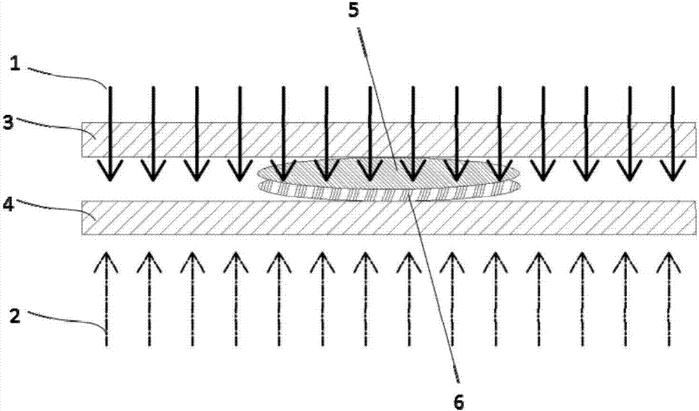
[0017] The hybrid bonding method of the prior art is introduced as follows: two silicon wafers that need to be bonded are provided, wherein the bonding interface of each silicon wafer contains both metal and insulator; the bonding of the two silicon wafers After the interfaces are aligned, a bonding process and an annealing process are performed on the two silicon wafers. In the bonding process, two silicon wafers need to ...


PUM


Abstract

The invention discloses a method for improving the hybrid bonding strength of wafers. The method is characterized by comprising the steps of providing wafers which need to be bonded; and aligning bonding interfaces of the wafers and carrying out a bonding technology and a thermal annealing technology on the wafers, wherein the wafers are subjected to hot pressing in the process of the bonding technology, and the wafers are further pressurized in the process of the thermal annealing technology. After the method disclosed by the invention is used, the hybrid bonding strength can be effectively improved, and the caused product yield loss and hidden danger of scrapping are reduced.

Description

technical field [0001] The invention relates to a wafer hybrid bonding method, in particular to a method for improving the wafer hybrid bonding strength. Background technique [0002] Three-dimensional integrated circuits need to realize the internal interconnection of thousands of chips while bonding two wafers, and these require conductive bonding of two wafers. Generally, conductive connections can be achieved through simple metal bonding processes and The hybrid bonding process with higher bonding strength is realized. Since the strength achieved by the pure metal bonding process is not ideal, the hybrid bonding process is currently the first choice for the bonding process in 3D integrated circuits. [0003] The hybrid bonding technology is a bonding process in which a metal and an insulator are placed on the bonding interface of the wafer at the same time, and the metal on the bonding interface of the two wafers needs to be aligned with the metal during the bonding proc...

Claims


Application Information

Patent Timeline
Patent Type & Authority Applications(China)
IPC IPC(8): H01L21/18H01L21/324
CPCH01L21/187H01L21/324
Inventor 丁滔滔郭帅王家文王孝进王家友李春龙邢瑞远
Owner YANGTZE MEMORY TECH CO LTD
Why Eureka
Try Eureka