
Test method of bottom defect etched by hard mask

An inspection method and hard mask technology, applied in the direction of electrical components, circuits, semiconductor/solid-state device testing/measurement, etc., can solve the problems of low reference value, difficulty in scanning and observation, and inability to reflect intuitively, so as to improve the process Condition, simple operation effect

Active Publication Date: 2018-05-04
YANGTZE MEMORY TECH CO LTD
View PDF3 Cites 0 Cited by
  • Summary
  • Abstract
  • Description
  • Claims
  • Application Information

AI Technical Summary

Problems solved by technology

On the one hand, although it is easy to scan the defects on the etched surface of the hard mask, it cannot intuitively reflect whether it will affect the subsequent deep hole etching, and the reference value of the defect results is not high; on the other hand, the bottom of the hard mask etched Whether it is completely opened or not and the uniformity of the pore diameter will directly affect the result of deep hole etching. The ratio is also relatively high, so it is difficult to directly scan and observe the bottom defects

Method used


Image

  • Test method of bottom defect etched by hard mask
  • Test method of bottom defect etched by hard mask
  • Test method of bottom defect etched by hard mask

Examples


Embodiment Construction

[0024] Exemplary embodiments of the present disclosure will be described in more detail below with reference to the accompanying drawings. Although exemplary embodiments of the present disclosure are shown in the drawings, it should be understood that the present disclosure may be embodied in various forms and should not be limited by the embodiments set forth herein. Rather, these embodiments are provided for more thorough understanding of the present disclosure and to fully convey the scope of the present disclosure to those skilled in the art.

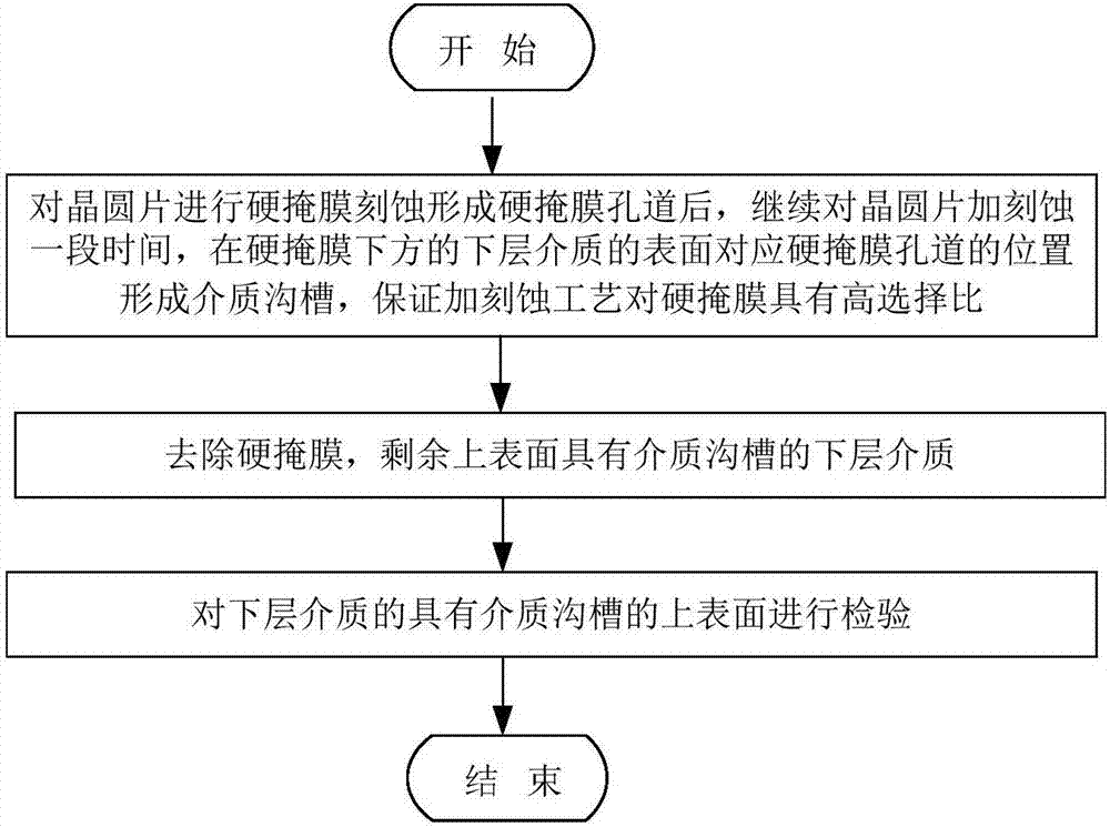
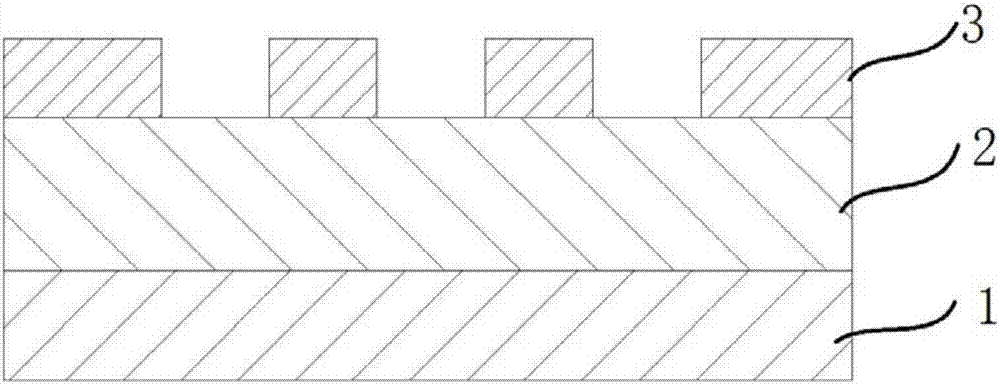
[0025] The basic idea of ​​the present invention is to continue to etch the wafer for a period of time after the etching of the hard mask is completed, so that the upper surface of the lower layer dielectric forms a dielectric groove corresponding to the position of the hole of the hard mask. Due to factors such as blockage in the hard mask etching, the etching will be stopped, that is, if the hard mask channel cannot be fully opene...


PUM


Abstract

The invention relates to a test method of a bottom defect etched by a hard mask, which includes steps of etching a hard mask to form a hard mask duct and then eroding a wafer piece for a period of time; forming a medium channel on the surface of a lower medium corresponding to the hard mask duct, guaranteeing that the etching process has high selectivity ratio to the hard mask; removing the hard mask, remaining the lower medium of which upper surface has the medium channel; testing the upper surface with the medium channel of the lower medium. The test method can exactly and intuitionally reflect the existence of the hard mark etching, and is convenient to timely and exactly improve the technical condition and lays a good foundation for the subsequent process.

Description

technical field [0001] The invention relates to the field of semiconductor manufacturing technology, in particular to a method for inspecting bottom defects of hard mask etching. Background technique [0002] In the preparation process of 3D NAND flash memory, the upper hard mask needs to be etched before the deep hole etching. After the hard mask is etched, whether the channel is completely opened, that is, whether the bottom is in contact with the underlying medium, determines the subsequent deep hole. Whether the etching can be carried out, and the uniformity of the hole diameter at the bottom of the hard mask channel and the roundness of the hole will also directly affect the morphology of the deep hole etching. Therefore, it is of great significance to investigate the defect problem at the bottom of hard mask etching for subsequent deep hole etching. [0003] In the existing process flow of deep hole etching, the defects of the process are scanned and observed after th...

Claims


Application Information

Patent Timeline
Patent Type & Authority Applications(China)
IPC IPC(8): H01L21/66
CPCH01L22/12H01L22/20
Inventor 肖为引王猛陈保友黄海辉刘隆冬苏恒朱喜峰
Owner YANGTZE MEMORY TECH CO LTD
Learn More