Curved surface image sensor, and welding structure of circuit board and camera module thereof

An image sensor and welding structure technology, applied in the field of photography, can solve problems such as unfavorable thinning of the camera module, difficult design, and 3' length of the binding wire, etc., and achieves the effect of small space, light and thin, and simplified design.

Inactive Publication Date: 2018-05-04
TRULY OPTO ELECTRONICS
View PDF5 Cites 3 Cited by
  • Summary
  • Abstract
  • Description
  • Claims
  • Application Information

AI Technical Summary

Problems solved by technology

However, if figure 1 As shown, the first welding PAD 11' on the curved surface image sensor 1' still follows the design of the planar image sensor and is arranged on its photosensitive surface, which causes it to be bound to the second welding PAD

Method used


Image

  • Curved surface image sensor, and welding structure of circuit board and camera module thereof
  • Curved surface image sensor, and welding structure of circuit board and camera module thereof
  • Curved surface image sensor, and welding structure of circuit board and camera module thereof

Examples


Example Embodiment

[0022] Example one

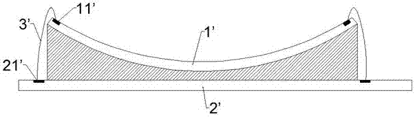
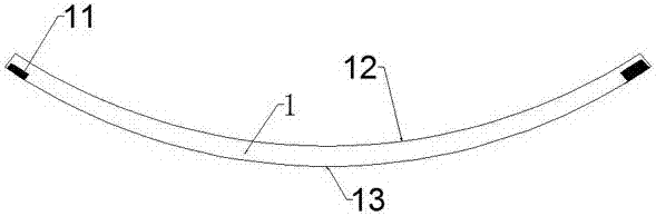
[0023] Such as figure 2 As shown, a curved image sensor 1 includes a photosensitive surface 12 and a welding surface 13 opposite to each other. The photosensitive surface 12 is a concave curved surface, and the welding surface 13 is a convex curved surface and is provided with at least one first welding PAD 11.

[0024] Depending on the welding method between the curved image sensor 1 and the circuit board 2, the first welding PAD 11 can be arranged at any position on the welding surface 13, but for the convenience of welding, the first welding PAD 11 is preferably Set on the edge of the welding surface 13.

Example Embodiment

[0025] Example two

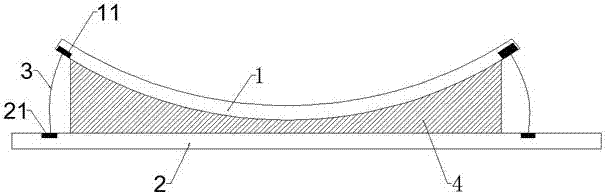
[0026] Such as Figure 3-5 As shown, a welding structure of a curved image sensor 1 and a circuit board 2 includes a circuit board 2, a curved base 4, and the above-mentioned curved image sensor 1, from bottom to top. The circuit board 2 faces the curved image sensor 1 At least one second welding PAD 21 is provided on one surface; the curved base 4 includes a bottom surface and a top surface opposite to each other, the bottom surface of which is a flat surface for mounting it on the circuit board 2, and the top surface is concave The curved surface is used to set the welding surface 13 of the curved image sensor 1; there is a one-to-one correspondence between the first welding PAD 11 on the curved image sensor 1 and the second welding PAD 21 on the circuit board 2 connection.

[0027] The welding structure moves the first welding PAD 11 of the curved image sensor 1 from the existing photosensitive surface 12 to the welding surface 13, facing the second weldin...

Example Embodiment

[0035] Example three

[0036] A camera module includes the welding structure of the curved image sensor 1 and the circuit board 2 described in the second embodiment.


PUM


Abstract

The invention discloses a curved surface image sensor, and a welding structure of a circuit board and a camera module thereof. The curved surface image sensor comprises a photosensitive surface and awelding surface, which are opposite to each other, wherein the photosensitive surface is an inward concave curved surface, and the welding surface is an outward convex surface and is provided with atleast a first welding PAD. When the surface image sensor is electrically connected with the circuit board, it has the advantages of short connection distance, small connection impedance, low impedanceloss, and low design difficulty and the like, and the occupied space is small, which is beneficial to the light weight and thinness of the camera module.

Description

technical field [0001] The invention relates to the field of imaging, in particular to a curved surface image sensor, its welding structure with a circuit board, and a camera module. Background technique [0002] With the development of image sensor technology, major manufacturers have released their own curved image sensors one after another. Because the photosensitive surface of the curved image sensor is curved, it is closer to the retina, which is also a curved surface, so the imaging effect is closer to the human eye. It is an important development trend of future camera technology. However, if figure 1 As shown, the first welding PAD 11' on the curved surface image sensor 1' still follows the design of the planar image sensor and is arranged on its photosensitive surface, which causes it to be bound to the second welding PAD 21' on the circuit board 2'. When the wire 3' is soldered, there are problems such as long binding wire 3', high impedance loss, and difficult d...

Claims


Application Information

Patent Timeline
IPC IPC(8): H04N5/225
CPCH04N23/54H04N23/00
Inventor 花亚红
Owner TRULY OPTO ELECTRONICS
Why Eureka
Try Eureka