Integrated module, design method thereof and mobile terminal

A technology of integrated modules and design methods, applied in CAD circuit design, calculation, special data processing applications, etc., can solve the problems of low module welding yield and difficulty in miniaturized module production

Inactive Publication Date: 2018-05-11
NUBIA TECHNOLOGY CO LTD
View PDF11 Cites 0 Cited by
  • Summary
  • Abstract
  • Description
  • Claims
  • Application Information

AI Technical Summary

Problems solved by technology

[0003] The technical problem to be solved by the present invention is: due to the existing modular production technology, due to the limitation of the number of pins and the size of the pad, the soldering yield of the module is low, and it is also difficult to realize the problem of miniaturization of the module. This technical problem provides an integrated module and its design method, mobile terminal

Method used


Image

  • Integrated module, design method thereof and mobile terminal
  • Integrated module, design method thereof and mobile terminal
  • Integrated module, design method thereof and mobile terminal

Examples


no. 1 example

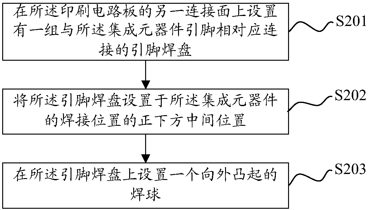
[0052] The design method of the integrated module provided by the embodiment of the present invention is applicable to various mobile terminals, including PCs, mobile phones, tablets, notebooks and other terminals. For details, please refer to figure 2 , figure 2 The basic flow chart of the design method of the integrated module provided in this embodiment, wherein the integrated module includes a printed circuit board and an integrated component, and the integrated component is soldered on a connecting surface of the printed circuit board; the design method include:

[0053] S201. A set of pin pads corresponding to the pins of the integrated component are provided on the other connecting surface of the printed circuit board.

[0054] S202. Set the pin pad at a middle position directly below the welding position of the integrated component.

[0055] S203. A solder ball protruding outward is arranged on the pin pad.

[0056] In the present embodiment, when the pin pads are arranged i...

no. 2 example

[0077] Figure 4 This is a schematic structural diagram of the integrated module provided by the second embodiment of the present invention. As shown in the figure, the integrated module 3 includes integrated components 31 and a printed circuit board 32, wherein the printed circuit board 32 includes a pin setting surface 321 and The device mounting surface 322, the integrated component 31 is soldered on the device mounting surface 322 of the printed circuit board 32.

[0078] A set of pin pads 1 are provided on the pin setting surface 321 of the printed circuit board 32, wherein the pin pads 1 are respectively connected to the pins in the integrated component 31.

[0079] The setting position of the pin pad 1 is located in the middle position directly below the welding position of the integrated component 31, and a solder ball 10 protruding outward is also provided on the pin pad.

[0080] In practical applications, in order to further reduce the footprint of the pin pad 1 on the pri...

no. 3 example

[0088] Please refer to Figure 5 , Figure 5 This is a schematic structural diagram of a mobile terminal provided by the third embodiment of the present invention. The mobile terminal includes at least one integrated module 3, which is specifically the integrated module provided in the above embodiment, and the integrated module 3 includes integrated components 31 And printed circuit board 32, where:

[0089] The integrated component 31 is soldered on one connecting surface of the printed circuit board 32, and a set of leads corresponding to the pins of the integrated component 31 are provided on the other connecting surface of the printed circuit board 32. Foot pad 1;

[0090] The setting position of the pin pad 1 is located in the middle position directly below the welding position of the integrated component 31, and a solder ball 10 protruding outward is also provided on the pin pad 1.

[0091] In this embodiment, when the pin pads 1 are set, they can be evenly distributed in the...


PUM


Abstract

The invention discloses an integrated module, a design method thereof and a mobile terminal. According to the method, when pin pads on a printed circuit board are arranged, the pin pads are arranged at middle positions which are directly under a welding position of the integrated module on the printed circuit board, and an outwardly protruding solder ball is also arranged on each pin pad; the solder-paste non-contact problem caused by a certain single-board deformation amount can be overcome through changing and arranging the pin pads to the positions which are directly under the printed circuit board and adding the solder balls, welding yield is higher as compared with that of an existing QFN package, thus the problems that in the prior art, the sizes of pin pads cannot be changed, and welding yield is lower are solved; and at the same time, the middle positions of the printed circuit board are effectively utilized through arranging the module by a manner provided by the invention, the arrangement positions of the pads are enabled to be changeable and the sizes are enabled to be adjustable, the size of the printed circuit board is further reduced, and miniaturized design of the module is realized.

Description

Technical field [0001] The present invention relates to the field of terminal technology, and more specifically, to an integrated module and a design method thereof, and a mobile terminal. Background technique [0002] With the continuous development of integration technology, especially small functional modules, in order to facilitate production and installation, most of the functions currently tend to be modularized. Modularized production is conducive to the control of production costs. However, in the existing technology, Most of the output pin settings on the module PCB are set at the peripheral edge of the PCB board, and the middle area of ​​the PCB board is not effectively used, which leads to the unreasonable layout of the components on the module. At the same time, through the current module production method, due to the number of output pins of the module, the QFN-type bottom pad size pin soldering yield requirement is restricted (the flat-bottom package is separated fr...

Claims


Application Information

Patent Timeline
Patent Type & Authority Applications(China)
IPC IPC(8): G06F17/50
CPCG06F30/39
Inventor 郑锐
Owner NUBIA TECHNOLOGY CO LTD
Why Eureka
Try Eureka