Display panel and production method thereof

A technology for display panels and manufacturing methods, applied in semiconductor/solid-state device manufacturing, electrical components, electric solid-state devices, etc., can solve problems such as lowering the production yield of AMOLED display panels, cracking or cracks, and AMOLED display panel production failures, to achieve The effect of reducing difficulty, alleviating stress concentration, and improving production yield

Inactive Publication Date: 2018-05-11
WUHAN CHINA STAR OPTOELECTRONICS SEMICON DISPLAY TECH CO LTD
View PDF6 Cites 23 Cited by
  • Summary
  • Abstract
  • Description
  • Claims
  • Application Information

AI Technical Summary

Problems solved by technology

In the cutting process of AMOLED display panels, since the cut film layer is mostly composed of inorganic films such as SiNx and SiOx, and the inorganic film layer is thick, it is easy to generate stress accumulation during the cutting process, thus causing cracks in the cut film layer Or cracks, if the cracks spread to the packaging area or peripheral wiring area or display area of ​​the AMOLED display panel, it will lead to the failure of the AMOLED display panel production and reduce the production yield of the AMOLED display panel

Method used


Image

  • Display panel and production method thereof
  • Display panel and production method thereof
  • Display panel and production method thereof

Examples


Embodiment Construction

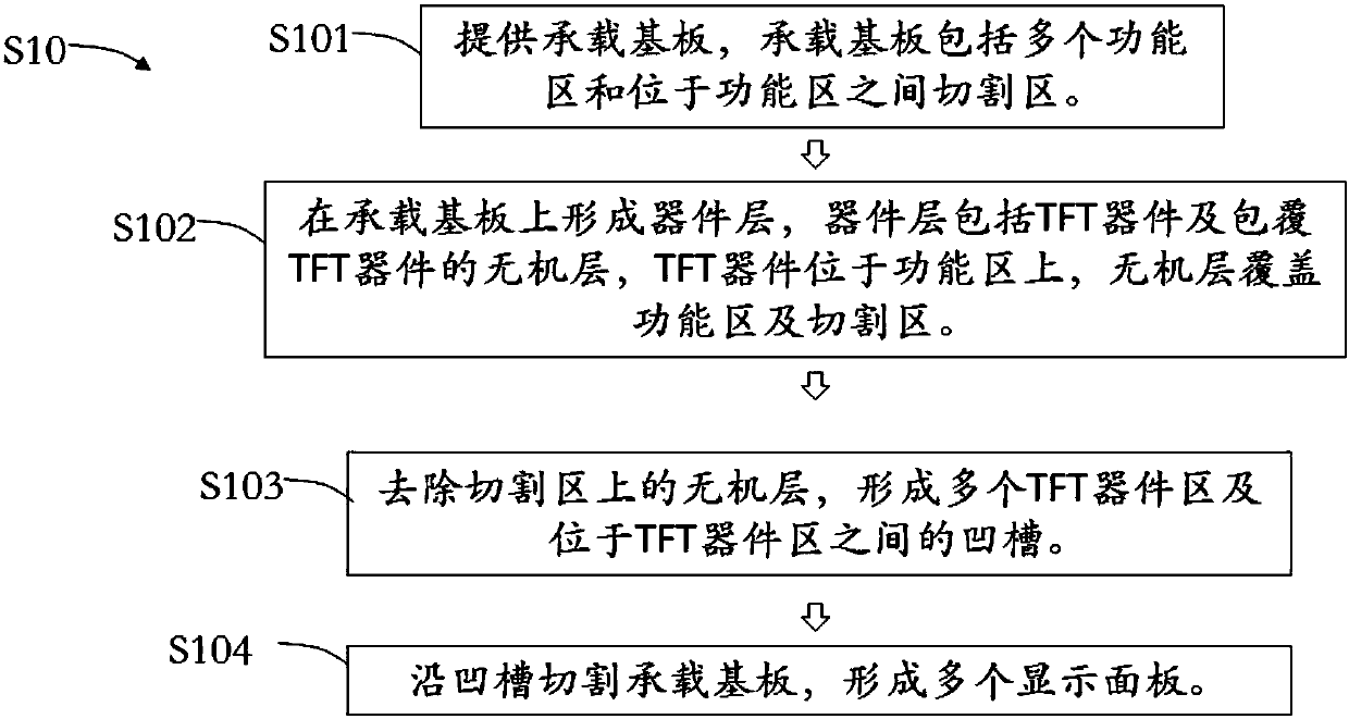
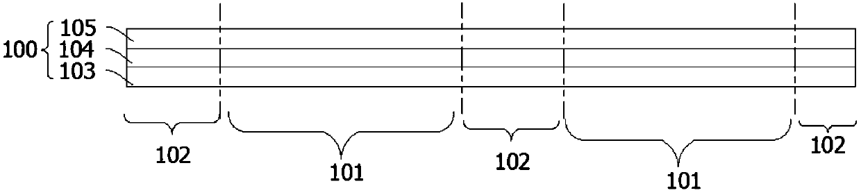
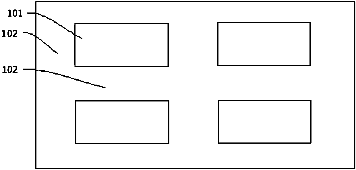
[0036] In order to more clearly understand the above objects, features and advantages of the present application, the present application will be described in detail below in conjunction with the accompanying drawings and specific embodiments. It should be noted that, in the case of no conflict, the embodiments of the present application and the features in the embodiments can be combined with each other.

[0037] A lot of specific details are set forth in the following description to facilitate a full understanding of the application, and the described implementations are only a part of the implementations of the application, but not all of the implementations. Based on the implementation manners in this application, all other implementation manners obtained by persons of ordinary skill in the art without making creative efforts belong to the scope of protection of this application.

[0038] In addition, the following descriptions of the various embodiments refer to the attac...


PUM


Abstract

The invention provides a production method of a display panel. The production method comprises the following steps of providing a bearing substrate, wherein the bearing substrate comprises a pluralityof functional areas and cutting areas located between the functional areas; forming a device layer on the bearing substrate, wherein the device layer comprises a TFT device and an inorganic layer coating the TFT device; the TFT device is located on the functional areas; and the inorganic layer covers the functional areas and the cutting areas; removing the inorganic layer on the functional areasand forming a plurality of TFT device areas and grooves located between the TFT device areas; and cutting the bearing substrate along the grooves and forming a plurality of display panels. The invention further provides the display panel. The production yield of the display panel can be improved.

Description

technical field [0001] The invention relates to the field of display technology, in particular to a display panel and a manufacturing method thereof. Background technique [0002] Active-matrix organic light emitting diode display panel (Active-matrix organic light emitting diode, referred to as AMOLED), has the characteristics of self-illumination, wide viewing angle, high color saturation, especially its low driving voltage and low power consumption, and fast response , light weight, thin thickness, simple structure, low cost, etc., is regarded as one of the most promising display products. [0003] In the manufacturing process of the AMOLED display panel, in order to reduce the production cost, a plurality of display panels are manufactured on a large substrate to form a display panel motherboard, and then the display panel motherboard is cut into individual display panel units. In the cutting process of AMOLED display panels, since the cut film layer is mostly composed ...

Claims


Application Information

Patent Timeline
Patent Type & Authority Applications(China)
IPC IPC(8): H01L21/78H01L21/311H01L27/32
CPCH01L21/31111H01L21/78H10K59/12
Inventor 易士娟
Owner WUHAN CHINA STAR OPTOELECTRONICS SEMICON DISPLAY TECH CO LTD
Why Eureka
Try Eureka