Flexible packaging structure and preparation method thereof, and wearable equipment

A flexible packaging and packaging structure technology, which is applied in semiconductor/solid-state device manufacturing, electrical components, electrical solid-state devices, etc., can solve the problem that flexible packaging substrates and flexible circuit boards are not effectively used, and meet the requirements of ensuring signal integrity. The effect of improving package integration

Active Publication Date: 2018-05-11
SANECHIPS TECH CO LTD
View PDF7 Cites 6 Cited by
  • Summary
  • Abstract
  • Description
  • Claims
  • Application Information

AI Technical Summary

Problems solved by technology

However, in the existing chip packaging process, in many cases, the hard substrate is connected to the peripheral application circuit wiring. In this way, the integrated circuit chip is made of hard material, and the flexible packaging substrate and flexible circuit board are not effectively utilized.

Method used


Image

  • Flexible packaging structure and preparation method thereof, and wearable equipment
  • Flexible packaging structure and preparation method thereof, and wearable equipment
  • Flexible packaging structure and preparation method thereof, and wearable equipment

Examples


Embodiment 1

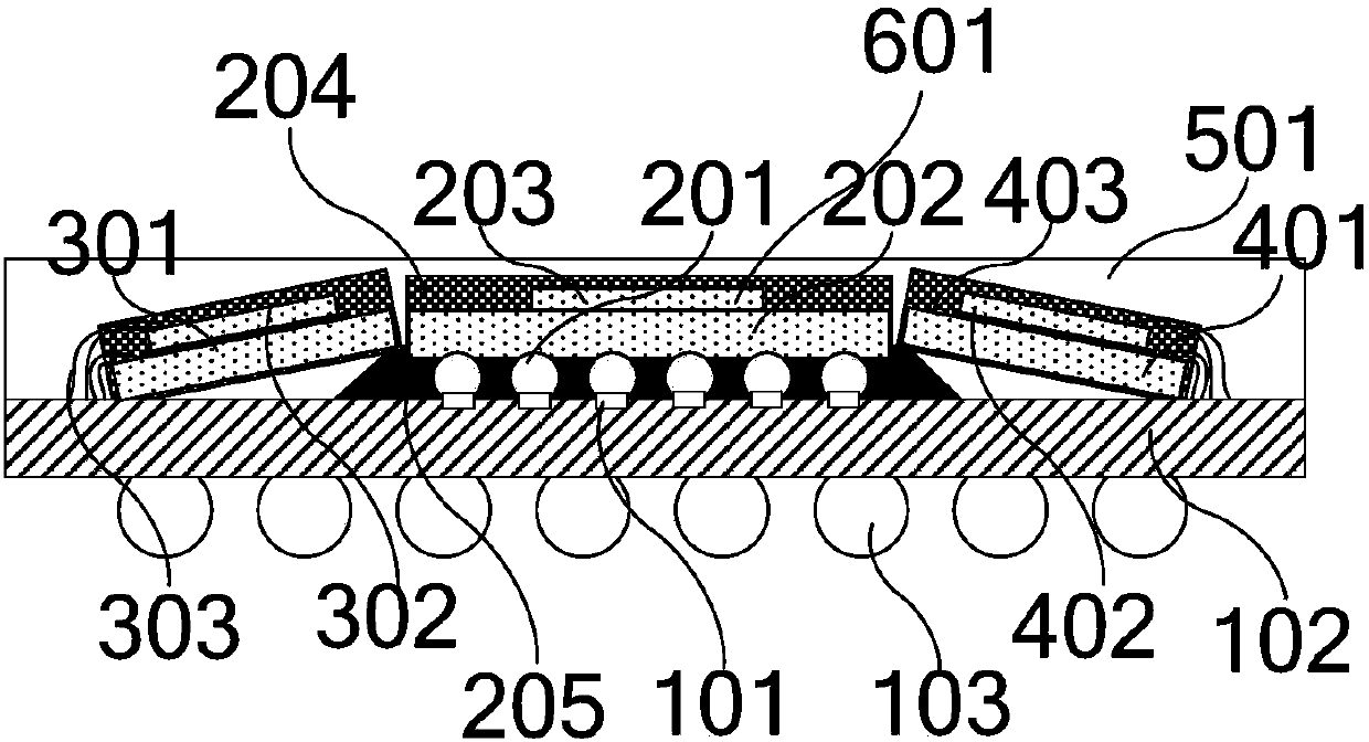
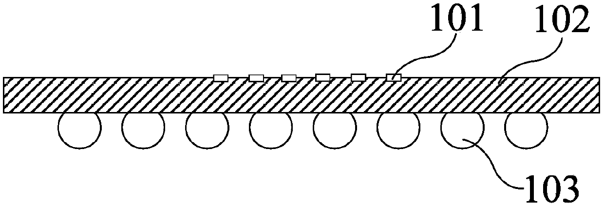
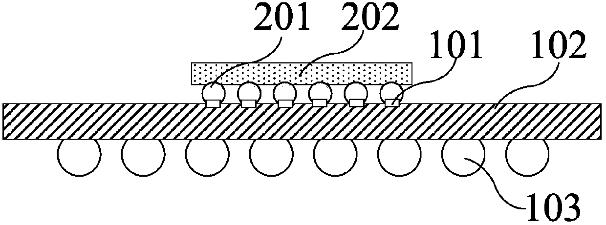
[0033] This embodiment provides a flexible packaging structure. Specifically, in order to solve the problem that the existing multi-chip packaging technology does not meet the flexible feature requirements of integrated chips, and multi-chip tiles occupy too much substrate area, the flexible packaging structure described in this embodiment The multi-chip packaging structure specifically includes: a flexible packaging substrate, a first rigid package, and at least one second rigid package; the first rigid package includes at least one first chip, and is used to cover the at least one first A hard encapsulation material for the chip; the second hard package includes: at least one third chip, and a hard encapsulation material for covering the at least one third chip; the first hard package and the At least one second rigid package is placed on the upper surface of the flexible packaging substrate; wherein, the package structure further includes: a flexible encapsulation material; ...

Embodiment 2

[0060] This embodiment provides a method for manufacturing the flexible packaging structure described in Embodiment 1 above; specifically, the method includes:

[0061] At least a first rigid package and at least one second rigid package are arranged on the upper surface of the flexible package substrate; the first rigid package includes at least one first chip, and a cover for covering the at least one first chip A hard encapsulation material; the second hard package includes: at least one third chip, and a hard encapsulation material for covering the at least one third chip;

[0062] At least the first rigid encapsulation and at least one second rigid encapsulation are encapsulated therein by a flexible encapsulation material.

[0063] Here, in order to meet the requirements of existing multi-chips, the first rigid package further includes at least one second chip; the at least one second chip is placed on the upper surface of the at least one first chip; and / or, The second...


PUM


Abstract

The invention discloses a flexible packaging structure which comprises a flexible packaging substrate, a first hard packaging body and at least one second hard packaging body; the first hard packagingbody comprises at least one first chip and a hard packaging material for wrapping the at least one first chip; the second hard packaging body comprises at least one third chip and a hard packaging material for wrapping the at least one third chip; and the first hard packaging body and the at least one second hard packaging body are arranged in the upper surface of the flexible packaging substrate. A flexible packaging material is further included, and packages the first and second hard packaging bodies at least. The invention also discloses a preparation method of the flexible packaging structure and wearable equipment.

Description

technical field [0001] The invention relates to semiconductor device packaging technology, in particular to a packaging structure, a preparation method thereof, and a wearable device. Background technique [0002] Driven by the continuous development of electronic products in the direction of miniaturization, portability, multi-function, high integration and high reliability, integrated circuits are also developing in the direction of integration, miniaturization and modularization. In recent years, with the rise of smart wearable devices such as smart bracelets, smart sports shoes, and smart glasses, integrated circuits increasingly need to meet the needs of softness and bendability to fit the user's contours, so as to increase user experience and Improve the accuracy of data collected by equipment. Among them, the flexible packaging technology of integrated circuits can provide a stable and reliable working environment for integrated circuit chips, and play an important r...

Claims


Application Information

Patent Timeline
IPC IPC(8): H01L23/31H01L21/56
Inventor 张瑾
Owner SANECHIPS TECH CO LTD
Why Eureka
Try Eureka