Metal oxide semiconductor transistor and manufacturing method thereof

A technology of oxide semiconductors and manufacturing methods, which is applied in the direction of transistors, semiconductor/solid-state device manufacturing, semiconductor devices, etc., and can solve problems that affect device reliability, increase device on-resistance, and large leakage

Inactive Publication Date: 2018-05-18
SHENZHEN JINGTE INTELLIGENT MFG TECH CO LTD
View PDF2 Cites 0 Cited by
  • Summary
  • Abstract
  • Description
  • Claims
  • Application Information

AI Technical Summary

Problems solved by technology

However, one of the main problems currently faced by the current fabrication methods of metal-oxide-semiconductor (MOS) transistors is that as the feature size of the device shrinks (gate width), the length of the channel becomes shorter and shorter, and the same Under the concentration of the well region, the shorter the channel length, the easier it is for the source and drain to punch through, resulting in greater leakage, which affects the reliability of the device
If a multi-gate structure is adopted, the channel length will increase significantly, but it will inevitably lead to an increase in channel resistance and an increase in the on-resistance of the device, thereby affecting the reliability of the device.

Method used


Image

  • Metal oxide semiconductor transistor and manufacturing method thereof
  • Metal oxide semiconductor transistor and manufacturing method thereof
  • Metal oxide semiconductor transistor and manufacturing method thereof

Examples


Embodiment Construction

[0023] The following will clearly and completely describe the technical solutions in the embodiments of the present invention. Obviously, the described embodiments are only some of the embodiments of the present invention, rather than all the embodiments. Based on the embodiments of the present invention, all other embodiments obtained by persons of ordinary skill in the art without making creative efforts belong to the protection scope of the present invention.

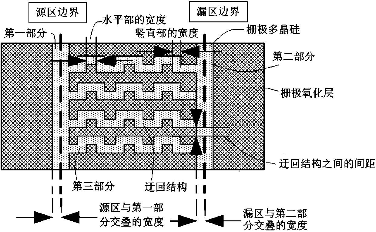
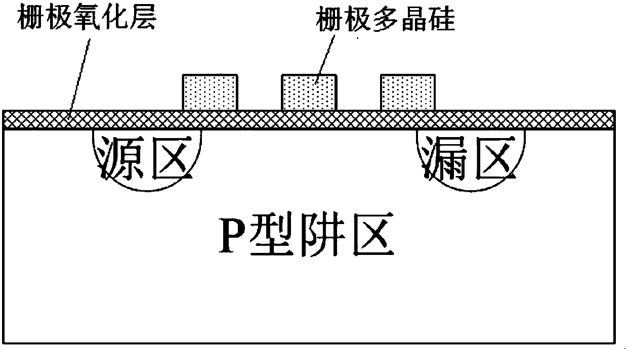
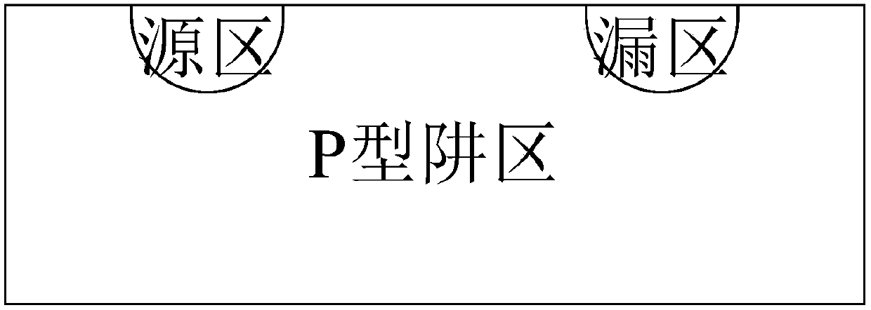
[0024] see Figure 1-Figure 2 , figure 1 is a partial plan view of the metal oxide semiconductor transistor according to the first embodiment of the present invention, figure 2 yes figure 1 A schematic cross-sectional view of a metal-oxide-semiconductor transistor is shown. The metal oxide semiconductor transistor includes a P-type well region, a source region and a drain region formed on the surface of the P-type well region, a gate formed on the source region and the drain region and on the P-type well region ...


PUM


Abstract

The present invention relates to a metal oxide semiconductor transistor. The metal oxide semiconductor transistor comprises a P-type well area, a source area and a drain area formed on the surface ofthe P-type well area, a gate oxide layer formed on the source area, the drain area and the P-type well area, and gate poly-silicon formed on the gate oxide layer. The gate poly-silicon comprises a first part at least partially located on the gate oxide layer of the source area, a second part at least partially located on the gate oxide layer of the drain area, and a third part connecting the firstpart and the second part. The third part comprises circuitous structure(s), and the length of the circuitous structure(s) is greater than the distance between the first part and the second part.

Description

【Technical field】 [0001] The present invention relates to the technical field of semiconductor manufacturing technology, in particular, to a metal oxide semiconductor transistor and a manufacturing method thereof. 【Background technique】 [0002] Metal-oxide-semiconductor (MOS) transistors are basic devices in semiconductor manufacturing, and are widely used in various integrated circuits. However, one of the main problems currently faced by the current fabrication methods of metal-oxide-semiconductor (MOS) transistors is that as the feature size of the device shrinks (gate width), the length of the channel becomes shorter and shorter, and the same Under the concentration of the well region, the shorter the channel length, the easier it is for the source and drain to punch through, resulting in greater leakage, which affects the reliability of the device. If a multi-gate structure is adopted, the channel length will increase significantly, but it will inevitably lead to an i...

Claims


Application Information

Patent Timeline
Patent Type & Authority Applications(China)
IPC IPC(8): H01L29/423H01L29/10H01L29/78H01L21/336H01L21/28
CPCH01L29/1033H01L29/401H01L29/42376H01L29/4238H01L29/66568H01L29/78
Inventor 不公告发明人
Owner SHENZHEN JINGTE INTELLIGENT MFG TECH CO LTD
Why Eureka
Try Eureka