Methods for transistor formation using selective gate implantation

a gate implantation and selective technology, applied in the field of semiconductor devices, can solve the problems of increasing logic gate delay and processing time, reducing transistor drive current, and requiring large feature sizes, and achieve the effect of facilitating precise control of doping concentrations

Inactive Publication Date: 2009-08-11
TEXAS INSTR INC
View PDF11 Cites 1 Cited by
  • Summary
  • Abstract
  • Description
  • Claims
  • Application Information

AI Technical Summary

Benefits of technology

[0011]The selective implantation of the invention may be employed to provide enough doping so that poly depletion is minimized or mitigated for all layout variations. This may provide several advantages in the manufacture of semiconductor products, for example, those having various transistors of different sizes. In such a situation, poly depletion differences for transistors of different lengths and / or widths are no longer significant, due to the fact that poly depletion is much less of an issue overall. Another advantage is that the reduced poly depletion increases gate capacitance and therefore increases transistor drive current at a given off state leakage current. Thus, the various aspects of the invention may be employed to provide one or more advantages over existing techniques in the manufacture of semiconductor devices.
[0013]In one example illustrated and described below, a substantially conformal film, such as an oxide, is formed over the semiconductor device. The wafer is then planarized, such as using chemical mechanical polishing (CMP) to expose a portion of the gate structure, and the selective implantation is performed using the patterned oxide film as an implant mask. In another example, a substantially non-conformal spin-on or resist material is formed over the device, which may be etched to expose the gate structure, for instance, using a reactive ion etch process. Depending on the non-conformal nature of the film, no film may need to be removed between film formation and the selective gate implantation. The selective gate implantation thus provides extra dopants to the gate structure without significantly doping the source / drain regions of the substrate. Thereafter, the implantation mask may be removed, such as by wet or dry etching, for further processing of the wafer. The invention thus facilitates precise control over the doping concentrations and uniformity of both the source / drain regions of the substrate, as well as of the gate structure, allowing compensation for process related dopant depletion from the gate.

Problems solved by technology

In addition, although generally scaled to be smaller, certain devices require larger feature sizes than others, including gate dimensions.
The increase in the effective thickness of the gate oxide under the inversion condition has the effect of an increase in threshold voltage and reduction in gate capacitance, in turn causing a reduction in transistor drive current and increased logic gate delay and processing time.

Method used


Image

  • Methods for transistor formation using selective gate implantation
  • Methods for transistor formation using selective gate implantation
  • Methods for transistor formation using selective gate implantation

Examples


Embodiment Construction

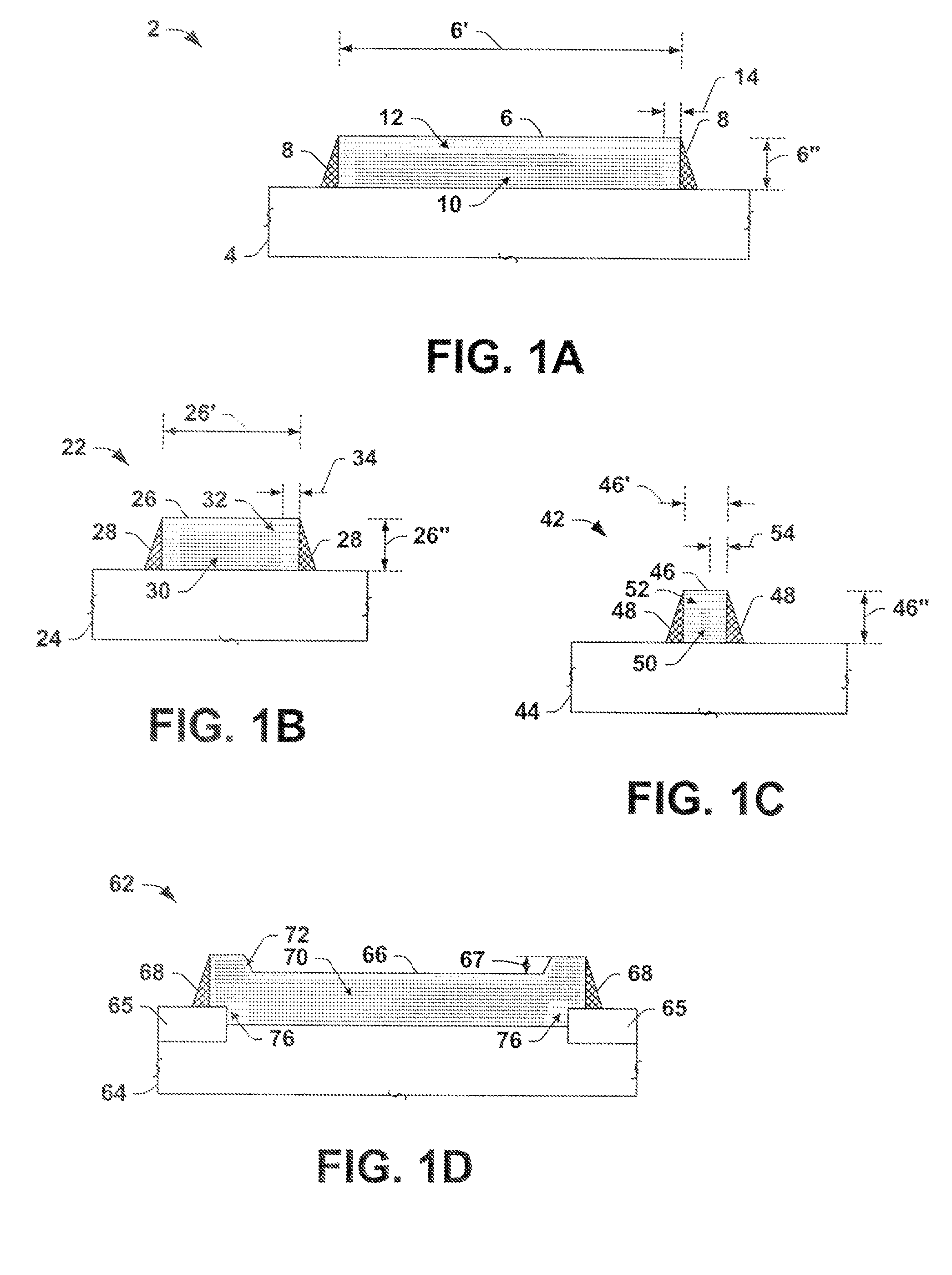
[0040]The present invention will now be described with reference to the attached drawings, wherein like reference numerals are used to refer to like elements throughout. Referring initially to FIGS. 1A-1D, a high degree of poly depletion occurs when an insufficient amount of dopant is introduced to the poly gate region nearest the gate oxide. This can be due to an insufficient amount of dopants being introduced to the polysilicon, or to the anneal subsequent to the doping of a poly gate being insufficient to drive the implanted impurities down the entire depth of the poly gate. Because the amount of dopant and the degree of annealing can be limited by other practical manufacturing considerations, such as dopant diffusion in other regions of the transistor structure, most often both of these factors contribute significantly.

[0041]Consequently, a portion of the poly gate nearest the underlying gate oxide is depleted of carriers and behaves as an insulating region. As a result, the tra...


PUM


Abstract

Methods are disclosed for semiconductor device fabrication in which dopants are selectively implanted into transistor gate structures to counteract or compensate for dopant depletion during subsequent fabrication processing. A patterned implant mask is formed over a semiconductor device, which exposes at least a portion of the gate structure and covers the remaining upper surfaces of the device. Thereafter, dopants are selectively implanted in to the exposed gate structure.

Description

RELATED APPLICATION[0001]This is a divisional application of Ser. No. 10 / 226,536 filed Aug. 23, 2002.[0002]This application is a Continuation-in-Part of Ser. No. 10 / 123,686, filed Apr. 16, 2002, which is entitled “METHODS FOR TRANSISTOR GATE FORMATION USING GATE SIDEWALL IMPLANTATION”.FIELD OF INVENTION[0003]The present invention relates generally to semiconductor devices and more particularly to methods for doping transistor gates in the manufacture of semiconductor devices.BACKGROUND OF THE INVENTION[0004]Field effect transistors (FETs) are widely used in the electronics industry for switching, amplification, filtering, and other tasks related to both analog and digital electrical signals. Most common among these are metal-oxide-semiconductor field-effect transistors (MOSFETs), wherein a doped polysilicon gate is energized to create an electric field within a semiconductor channel underlying the gate, by which current is allowed to conduct between doped source / drain regions formed...

Claims


Application Information

Patent Timeline
Patent Type & Authority Patents(United States)
IPC IPC(8): H01L21/8238H01L21/04H01L21/336H01L21/8234
CPCH01L21/28035H01L29/66545H01L29/7833H01L29/6659H01L29/6656
Inventor JOHNSON, F. SCOTTGRIDER, TADMCKEE, BENJAMIN P.
Owner TEXAS INSTR INC
Why Eureka
Try Eureka