Semiconductor-Based Gas Sensor Assembly for Detecting a Gas and Corresponding Production Method

a technology of gas sensor and semiconductor, applied in the direction of instruments, measurement devices, scientific instruments, etc., can solve the problems of gas signal attenuation, serious signal drift, and low capacitance formation in the corresponding gate stack, so as to improve the resolution, the effect of high sensitivity and high capacitance formed by the gas-sensitive structur

Inactive Publication Date: 2018-01-18
ROBERT BOSCH GMBH
View PDF3 Cites 0 Cited by
  • Summary
  • Abstract
  • Description
  • Claims
  • Application Information

AI Technical Summary

Benefits of technology

[0008]The present invention makes it possible that gases in harsh environments can be detected with high sensitivity in a low concentration range with a semiconductor-based gas sensor assembly producible in large numbers. This is achieved, in particular, by the “burying” of the sensitive read-out transistor, such that contaminations and signal drifts associated therewith are avoided. A particularly high sensitivity is achieved by the use of at least partly polarizable dielectric layers, in particular thin-film layers, in the gas-sensitive structure. Said layers may have permittivities that are approximately two orders of magnitude higher than those of customary gate materials from semiconductor technology, such as SiO2 or Al2O3, such that the gate capacitance increases by precisely this factor and the resolution increases. Furthermore, the gas dependence of the capacitance of the gas-sensitive structure itself can be used given a suitable mode of operation. That is to say that not only does the gate dielectric, for example the polarizable dielectric layer, act as a passive insulation layer through which the applied field punches toward the channel region, but the permittivity that changes greatly in a field- or gas-dependent manner additionally affects the channel current.
[0009]In comparison with the suspended gate concept described in the prior art, this has the advantage, in particular, that no air gap is necessary. The air gap has the consequence that the capacitance formed by the gas-sensitive structure, also referred to as gate capacitance, is reduced and the transmission of the signal of absorbed gas species is impaired. Moreover, complex flip-chip mounting is not necessary during processing, such that a high integrability / miniaturizability of the sensor is ensured since flip-chip mounting presupposes a correspondingly large, “handlable” chip geometry, such that a miniaturization of the semiconductor-based gas sensor is possible only to a limited extent.

Problems solved by technology

However, serious signal drifts may occur as a result of the direct spatial proximity of the electrode exposed to the gas and the relatively sensitive field effect transistor.
However, as a result of an air gap used between sensitive layer and corresponding electrode, a capacitance that forms in a corresponding gate stack becomes relatively low, as a result of which the gas signals are attenuated in particular to a great extent.

Method used


Image

  • Semiconductor-Based Gas Sensor Assembly for Detecting a Gas and Corresponding Production Method
  • Semiconductor-Based Gas Sensor Assembly for Detecting a Gas and Corresponding Production Method

Examples


first embodiment

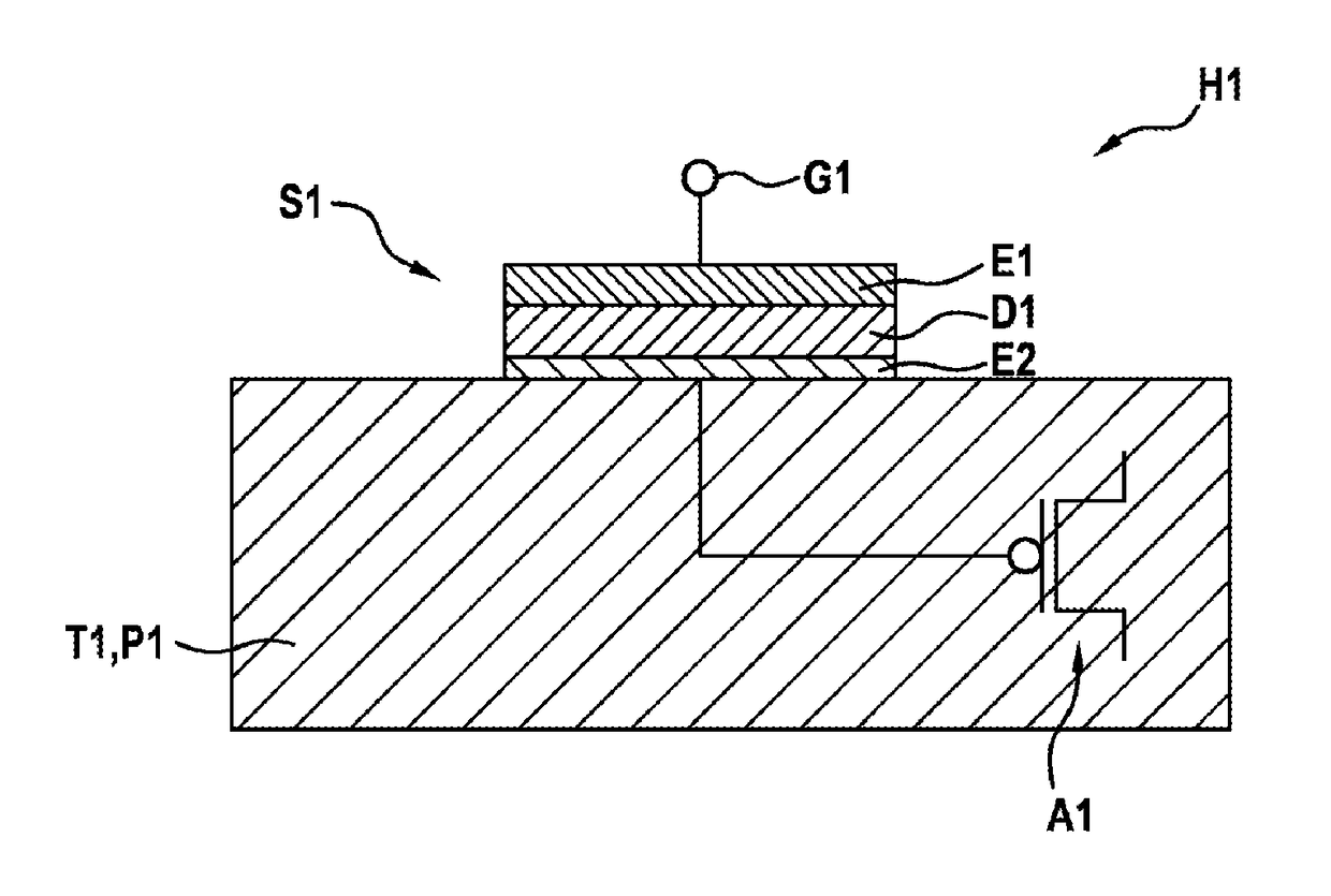
[0028]FIG. 1 shows a schematic perpendicular cross-sectional view for elucidating a semiconductor-based gas sensor assembly for detecting a gas and a corresponding production method in accordance with the present invention.

[0029]In FIG. 1, reference sign H1 denotes a semiconductor-based gas sensor assembly for detecting a gas. The semiconductor-based gas sensor assembly H1 comprises a gas-sensitive structure S1 comprising a gas electrode E1, an electrode E2 and an at least partly polarizable dielectric layer D1 arranged between the gas electrode E1 and the electrode E2. The gas-sensitive structure S1 is suitable for forming a capacitance during operation. Said capacitance of the gas-sensitive structure S1 is coupled to a gate G1 of a read-out sensor A1 and the read-out sensor A1 is situated in a substrate T1.

[0030]As shown in FIG. 1, in contrast to the suspended gate concept, there is no need for an air gap that reduces the gate capacitance and impairs the transmission of the signal...

second embodiment

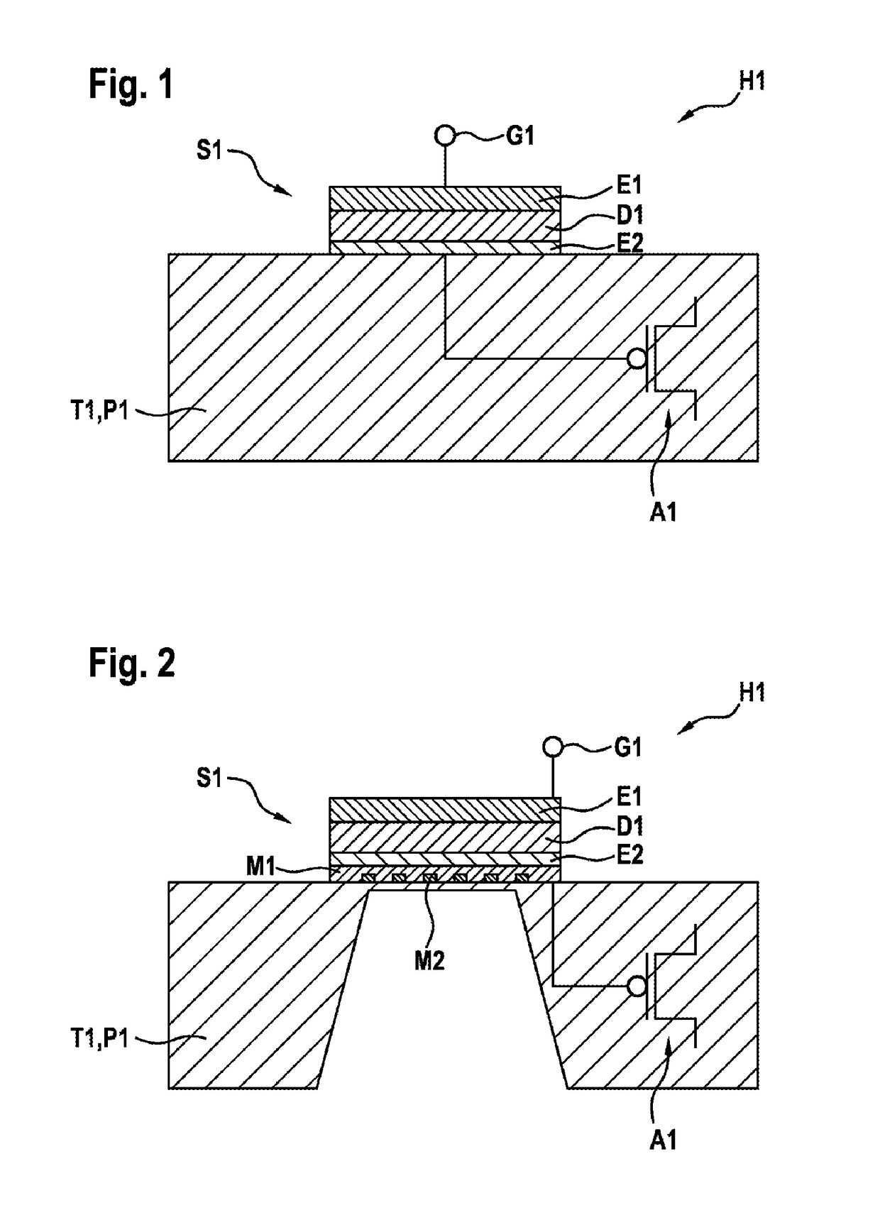
[0032]FIG. 2 shows a schematic perpendicular cross-sectional view for elucidating a semiconductor-based gas sensor assembly for detecting a gas and a corresponding production method in accordance with the present invention.

[0033]FIG. 2 shows the semiconductor-based gas sensor assembly H1 from FIG. 1 with the difference that the gas-sensitive structure S1 from FIG. 1 is arranged on a membrane M1 with an integrated heater M2. Furthermore, as shown in FIG. 2, a cutout is formed in the substrate T1 or the passivation layer P1 in the region of the gas-sensitive structure. In this case, the cutout is situated below the gas-sensitive structure S1 and is formed in the substrate T1 or the passivation layer P1. The cutout advantageously serves the purpose that the membrane is heated particularly rapidly by the integrated heating element on account of a thermal mass that is as small as possible, since a heat generated by the heating element does not have to be additionally emitted into or onto...


PUM

PropertyMeasurementUnit
temperaturesaaaaaaaaaa
polarizableaaaaaaaaaa
capacitanceaaaaaaaaaa

Abstract

A semiconductor-based gas sensor assembly for detecting a gas includes a gas-sensitive structure with a gas electrode, an electrode, and a dielectric layer, and also includes a readout transistor and a substrate. The dielectric layer is positioned between the gas electrode and the electrode, and is at least partially polarized. The readout transistor is positioned in or on the substrate, and includes a gate. The gas-sensitive structure is configured to form a capacitance that is coupled to the gate of the readout transistor.

Description

[0001]The present invention relates to a semiconductor-based gas sensor assembly for detecting a gas and a corresponding production method.PRIOR ART[0002]Gas sensors find diverse applications, a wide variety of physical and chemical measurement principles being used. In many areas of use, importance is increasingly being attached here to low costs, small structural size and low power consumption, with high demands being placed on the robustness of the gas sensors. Against this background, semiconductor-based components, in particular gas sensors, constitute an important alternative to electrochemical cells, for example.[0003]Field effect transistors (FET) having chemosensitive gate regions are known from the literature.[0004]DE 19849932 A1, DE 19814857 A1, WO 2005 / 075969 A1, DE 4239319 C2 and DE 19849932 A1 disclose so-called suspended gate FETs (SG-FETs). The latter relate to sensor concepts based on gas absorption and an associated change in potential or work function in the gate ...

Claims


Application Information

Patent Timeline
Patent Type & Authority Applications(United States)
IPC IPC(8): G01N27/414
CPCG01N27/4141
Inventor KUNZ, DENISSCHREIVOGEL, MARTIN
Owner ROBERT BOSCH GMBH
Why Eureka
Try Eureka