

A kind of semiconductor device and its manufacturing method, electronic device
A manufacturing method and semiconductor technology, applied in the direction of semiconductor devices, semiconductor/solid-state device manufacturing, electric solid-state devices, etc., to achieve the effects of increasing contact area, improving device power consumption, and increasing gate capacitance
- Summary
- Abstract
- Description
- Claims
- Application Information
AI Technical Summary
Problems solved by technology
Method used
Image

Examples
Embodiment 1
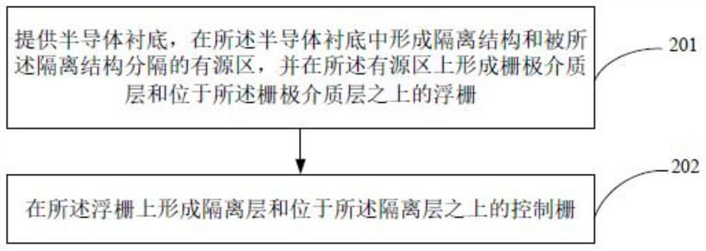
[0046] The following will refer to Figure 3A ~ Figure 3G A method for fabricating a semiconductor device according to an embodiment of the present invention will be described in detail. It can be understood that the flash memory includes not only the memory (cell) but also the peripheral area, and the manufacturing method of the semiconductor device in this embodiment is mainly aimed at the storage area of the flash memory, so in Figure 3A ~ Figure 3G Only a schematic cross-sectional view of the flash memory storage area is shown in , where Figure 3A ~ Figure 3G It is a cross-sectional view of a flash memory storage unit along the length direction of the floating gate. The so-called length direction of the floating gate refers to the direction perpendicular to the source and drain lines or the word line direction.
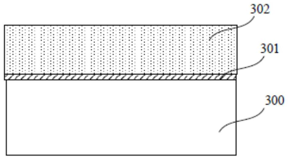
[0047] Firstly, a semiconductor substrate 300 is provided, and a gate dielectric layer 301 and a floating gate material layer 302 on the gate dielectric laye...
Embodiment 2
[0071] The present invention also provides a semiconductor device, such as Figure 4 As shown, the semiconductor device includes: a semiconductor substrate 400, an isolation structure 401 is formed in the semiconductor substrate 400 and an active region is separated by the isolation structure, and a gate dielectric is formed on the active region layer 402 and a floating gate 403 located on the gate dielectric layer 402; an isolation layer 404 and a control gate located on the isolation layer 404 are formed on the floating gate 403, wherein the floating gate 403 It includes a main body 4030 on the gate dielectric layer 402 and protrusions 4031 located at two ends of the main body 4030 and protruding toward the control gate.
[0072] Wherein, the semiconductor substrate 400 can be at least one of the materials mentioned below: Si, Ge, SiGe, SiC, SiGeC, InAs, GaAs, InP or other III / V compound semiconductors, and also include multiples composed of these semiconductors. The layer ...
Embodiment 3
[0080] Still another embodiment of the present invention provides an electronic device, including a semiconductor device and an electronic component connected to the semiconductor device. Wherein, the semiconductor device includes: a semiconductor substrate on which a floating gate is formed; a control gate is formed on the floating gate, wherein the floating gate includes a A main body and protrusions located at both ends of the main body and protruding toward the control grid.
[0081] Wherein, the semiconductor substrate can be at least one of the materials mentioned below: Si, Ge, SiGe, SiC, SiGeC, InAs, GaAs, InP or other III / V compound semiconductors, and multilayers composed of these semiconductors The structure or the like may be silicon-on-insulator (SOI), silicon-on-insulator (SSOI), silicon-germanium-on-insulator (S-SiGeOI), silicon-germanium-on-insulator (SiGeOI), and germanium-on-insulator (GeOI). Devices, such as NMOS and / or PMOS, can be formed on the semiconduc...
PUM
 Abstract
Description
Claims
Application Information