Fabrication method for inner-layer pattern of printed circuit board (PCB)

A technology of inner layer graphics and production methods, which is applied in the field of PCB board manufacturing, can solve the problems that it is difficult to eliminate the size deviation of film negatives, and the production process is difficult to realize continuous automatic production, so as to facilitate continuous and uninterrupted automatic production and improve precision. , to avoid the effect of size change

Inactive Publication Date: 2018-05-18
SHENZHEN KINWONG ELECTRONICS
View PDF7 Cites 5 Cited by
  • Summary
  • Abstract
  • Description
  • Claims
  • Application Information

AI Technical Summary

Problems solved by technology

[0003] The purpose of the present invention is to provide a method for making the inner layer pattern of the PCB board, aiming to solve the problem that the existing manufacturing process is difficult to eliminate the dimensional deviation caused by the size change of the film negative and the exposure alignment, and the traditional manufacturing process is difficult to realize continuous automation. production problem

Method used


Image

  • Fabrication method for inner-layer pattern of printed circuit board (PCB)

Examples


Embodiment Construction

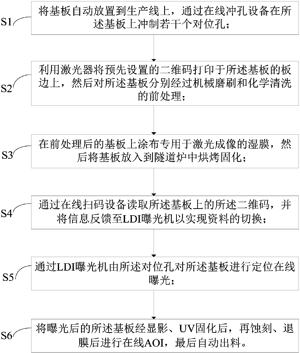
[0021] In order to make the object, technical solution and advantages of the present invention clearer, the present invention will be further described in detail below in conjunction with the accompanying drawings and embodiments. It should be understood that the specific embodiments described here are only used to explain the present invention, not to limit the present invention.

[0022] It should be noted that when an element is referred to as being “fixed” or “disposed on” another element, it may be directly on the other element or be indirectly on the other element. When an element is referred to as being "connected to" another element, it can be directly connected to the other element or indirectly connected to the other element.

[0023] It is to be understood that the terms "length", "width", "top", "bottom", "front", "rear", "left", "right", "vertical", "horizontal", "top" , "bottom", "inner", "outer" and other indicated orientations or positional relationships are b...


PUM


Abstract

The invention belongs to the field of manufacturing of a printed circuit board (PCB), and provides a fabrication method for an inner-layer pattern of the PCB. The fabrication method comprises the steps of sequentially performing document fabrication according to a two-dimensional code, performing on-line punching on a substrate, printing the two-dimensional code on the substrate by laser, pre-processing the substrate (including mechanical polishing-brushing and chemical cleaning), coating a wet film special for laser direct imaging (LDI), braking and curing the substrate coated with the wet film in a tunnel furnace, scanning the two-dimensional code, determining a type of a product, performing exposure, developing, uv curing, etching and film removal on connection line LDI, performing on-line automatic optic inspection (AOI), and finally, discharging a finished product. By the design, the problems that size deviation caused by size change and exposure alignment of a film is difficult to eliminate by an existing fabrication process and continuous and automatic production is difficult to achieve by a traditional fabrication process can be solved.

Description

technical field [0001] The invention belongs to the field of PCB board manufacturing, and in particular relates to a method for making inner layer graphics of a PCB board. Background technique [0002] At present, the inner layer graphics of the PCB board are made through a single pre-treatment (such as chemical cleaning), and then a common photosensitive wet film is coated on the board, and then exposed by a traditional exposure machine (such as a mercury lamp exposure machine), and then developed. , etching, and film removal are completed. This process cannot eliminate the dimensional deviation caused by the dimensional change of the film negative and the exposure alignment, so the quality of the product is difficult to control. In addition, when switching between PCB boards of different material numbers, it is necessary to manually replace the film, so continuous automatic production cannot be realized. Contents of the invention [0003] The purpose of the present inv...

Claims


Application Information

Patent Timeline
Patent Type & Authority Applications(China)
IPC IPC(8): H05K3/06
CPCH05K3/06H05K2203/052H05K2203/107
Inventor 付凤奇任城洵王海洋王俊
Owner SHENZHEN KINWONG ELECTRONICS
Why Eureka
Try Eureka