Touch substrate and its preparation method, touch panel
A substrate and touch technology, which is applied in the fields of instruments, calculations, electrical digital data processing, etc., can solve the problem of high incidence of dark line defects, reduce the incidence of dark line defects, facilitate implementation, and reduce production costs.
- Summary
- Abstract
- Description
- Claims
- Application Information
AI Technical Summary
Problems solved by technology
Method used
Image
Examples
no. 1 example
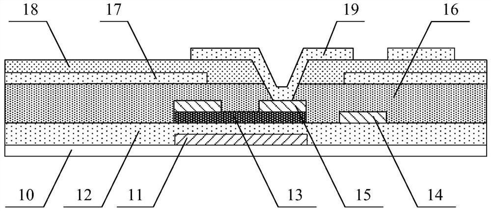
[0057] Figure 2A It is a schematic structural diagram of the display area of the first embodiment of the touch substrate of the present invention, Figure 2B It is a schematic structural diagram of the fan-out area of the first embodiment of the touch substrate of the present invention. Such as Figure 2A As shown, the display area of the touch control substrate includes: a gate electrode 11 disposed on a substrate 10, a first insulating layer 12 covering the gate electrode 11, an active layer 13 and a signal line 14 disposed on the first insulating layer 12, The source and drain electrodes 15 arranged on the active layer 13, the second insulating layer 16 covering the active layer 13, the signal line 14 and the source and drain electrodes 15, the touch electrode 17 arranged on the second insulating layer 16, covering the touch The third insulating layer 18 of the control electrode 17 and the pixel electrode 19 disposed on the third insulating layer 18 . Wherein, the...
no. 2 example
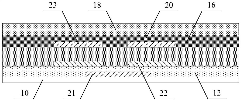
[0076] Figure 13 It is a schematic structural diagram of the second embodiment of the touch substrate of the present invention, illustrating the structure of the fan-out area. Such as Figure 13 As shown, this embodiment is a modification of the scheme of the aforementioned first embodiment, the structure of the display area is the same as that of the first embodiment, the difference is that the protective layer 20 set in the fan-out area is set on the third insulating layer 18 . Specifically, the fan-out area of the touch substrate includes: the gate lead-out line 21 arranged on the substrate 10, the first insulating layer 12 covering the gate lead-out line 21, the data lead-out line 22 arranged on the first insulating layer 12, covering The second insulating layer 16 of the data lead-out line 22 , the signal lead-out line 23 disposed on the second insulating layer 16 , the third insulating layer 18 covering the signal lead-out line 23 , and the protective layer 20 dispo...
no. 3 example
[0080] Figure 14A It is a schematic structural diagram of the display area of the third embodiment of the touch substrate of the present invention, Figure 14B It is a schematic structural diagram of the fan-out area of the third embodiment of the touch substrate of the present invention. Such as Figure 14A and Figure 14B As shown, this embodiment is a modification of the previous embodiment, the main structure is basically the same as the previous embodiment, the difference is that the protective layer 20 of this embodiment is arranged on the third insulating layer 18, and covers the entire substrate .
[0081] In this embodiment, the display area of the touch control substrate includes: a gate electrode 11 disposed on the substrate 10, a first insulating layer 12 covering the gate electrode 11, an active layer 13 and signal lines disposed on the first insulating layer 12 14. The source-drain electrodes 15 disposed on the active layer 13, the second insulating la...
PUM
 Abstract
Description
Claims
Application Information


