LED flip chip with controllable light-emitting angle, and electronic equipment employing same

A light-emitting angle and flip-chip technology, which is applied in the direction of circuits, electrical components, semiconductor devices, etc., can solve problems such as difficult to achieve backlight uniformity and small light-emitting angle of chips, so as to increase or decrease the light-emitting angle and change the light-emitting angle Effect

Pending Publication Date: 2018-06-05
ELEC TECH PHOTOELECTRIC TECH DALIAN
View PDF0 Cites 2 Cited by
  • Summary
  • Abstract
  • Description
  • Claims
  • Application Information

AI Technical Summary

Problems solved by technology

In some specific client applications, LEDs are required to have a wide range of light-emitting angles; for example, in the field of mobile phone backlight applications, it is difficult to achieve uniformity of the backlight due to the small light-emitting angle of the chip

Method used


Image

  • LED flip chip with controllable light-emitting angle, and electronic equipment employing same
  • LED flip chip with controllable light-emitting angle, and electronic equipment employing same
  • LED flip chip with controllable light-emitting angle, and electronic equipment employing same

Examples


Embodiment 1

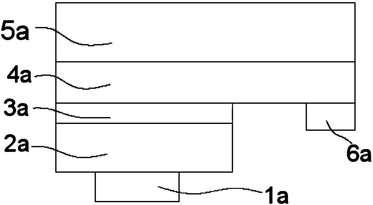
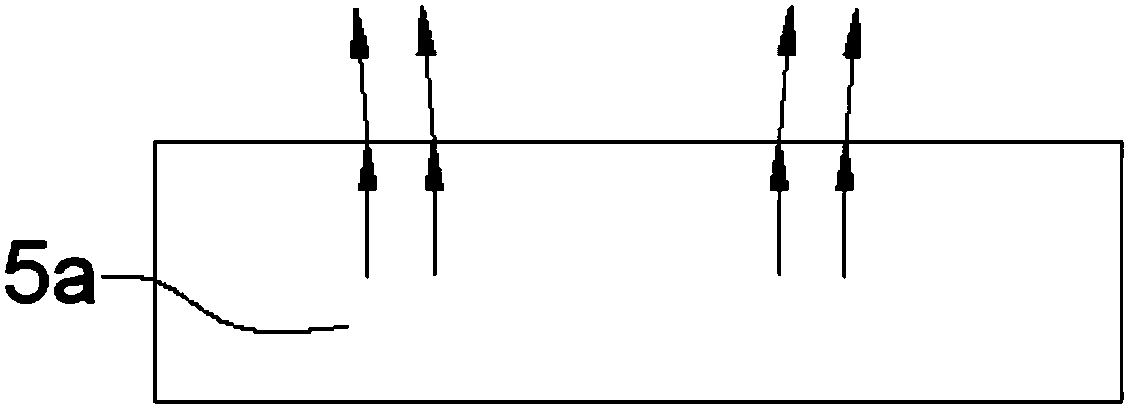
[0041] An LED flip-chip with a controllable luminous angle is applied to electronic equipment such as mobile phone backlight modules, backlight panel devices or electronic display devices. The electronic equipment is equipped with, for example, Figure 3 to Figure 5 , including a substrate 5, an N-type layer 4, a light-emitting layer 3 and a P-type layer 2, and from the substrate 5, the N-type layer 4, the light-emitting layer 3 and the P-type layer 2 are sequentially stacked in layers, And a P electrode 1 is provided on the P-type layer 2, and an N-electrode 6 is provided on the N-type layer 4. When emitting light, the light is directly emitted from the back of the flat substrate 5; the back surface of the substrate 5 is formed by laser ablation A single cross-sectional shape is a V-shaped plastic concave groove 7 that realizes controllable change of the light output angle through refraction.

[0042] continue as Figure 1 to Figure 3 , the depth of the single shaping recess...

Embodiment 2

[0047] Such as Figure 6 As shown, the difference between this embodiment and the first embodiment is that the cross-sectional shape is a circular arc-shaped plastic concave groove 7, and the shape of the opening of the plastic concave groove 7 on the substrate 5 is also circular, and the shape of the plastic concave groove 7 is circular. The first side wall 71 and the second side wall 72 of the shaping concave groove 7 are arc-shaped; the other structures are similar to those of the first embodiment, and will not be repeated here.

Embodiment 3

[0049] Such as Figure 7 and Figure 8 As shown, the difference between this embodiment and Embodiment 1 is that laser ablation is used on the back surface of the substrate 5 to form a plurality of plastics with the same size and shape and arranged in an array to realize controllable change of the light output angle through refraction. shaped recessed groove 7, and the cross-sectional shape of each shaped recessed groove 7 on the substrate 5 is V-shaped, a plurality of shaped recessed grooves 7 are arranged continuously, and two adjacent shaped recessed grooves 7 are formed on the substrate The openings on the 5 are connected.


PUM


Abstract

The invention provides an LED flip chip with a controllable light-emitting angle, and electronic equipment employing the same. The LED flip chip comprises a substrate, an N-type layer, a light-emitting layer and a P-type layer. The N-type layer, the light-emitting layer and the P-type layer are sequentially stacked from the substrate in a top-to-bottom manner. Moreover, the P-type layer is provided with an electrode P, and the N-type layer is provided with an electrode N. During light emitting, light directly comes out of the back surface of the flat substrate. The back surface of the substrate is provided with a single molded groove or more molded grooves through laser ablation, wherein the grooves are consistent in size and shape, are arranged in an array and achieve the controllable andchangeable light-outgoing angle through refraction. When light passes through the grooves on the surface of the substrate to propagate to the air, the light-outgoing angle is changed because of the refraction effect. The flip chip can achieve the change of the light-outgoing angle, thereby changing the light-outgoing angle.

Description

【Technical field】 [0001] The invention relates to the technical field of semiconductor optoelectronic chips, in particular to an LED flip-chip with controllable luminous angle. 【Background technique】 [0002] Generally, a light-emitting diode (Light-Emitting Diode, LED) is a semiconductor electronic component that can convert electricity into light, and can be widely used in displays, automotive lights, general lighting and other fields. Existing LED chips, especially flip chips, such as figure 1 and figure 2 As shown, generally, an N-type layer 4a, a light-emitting layer 3a, and a P-type layer 2a are stacked sequentially from top to bottom from the substrate 5a, and a P-type electrode 1a is arranged on the P-type layer 2a, and the N-type layer 4a is provided with an N electrode 6a. When emitting light, the light directly exits from the back of the flat substrate 5a, and the light is refracted at the cross section between the substrate 5a and the air, and the light exit a...

Claims


Application Information

Patent Timeline
Patent Type & Authority Applications(China)
IPC IPC(8): H01L33/20H01L33/22
CPCH01L33/20H01L33/22
Inventor 刘岩闫宝玉刘宇轩陈顺利丁逸圣
Owner ELEC TECH PHOTOELECTRIC TECH DALIAN
Why Eureka
Try Eureka