A kind of pull-up circuit for io circuit
A circuit and power supply technology, applied in logic circuits, logic circuit coupling/interfaces using field effect transistors, logic circuit interface devices, etc., can solve problems affecting the normal output of IO circuits
- Summary
- Abstract
- Description
- Claims
- Application Information
AI Technical Summary
Problems solved by technology
Method used
Image
Examples
Embodiment Construction
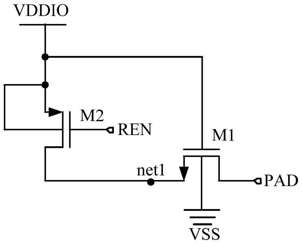
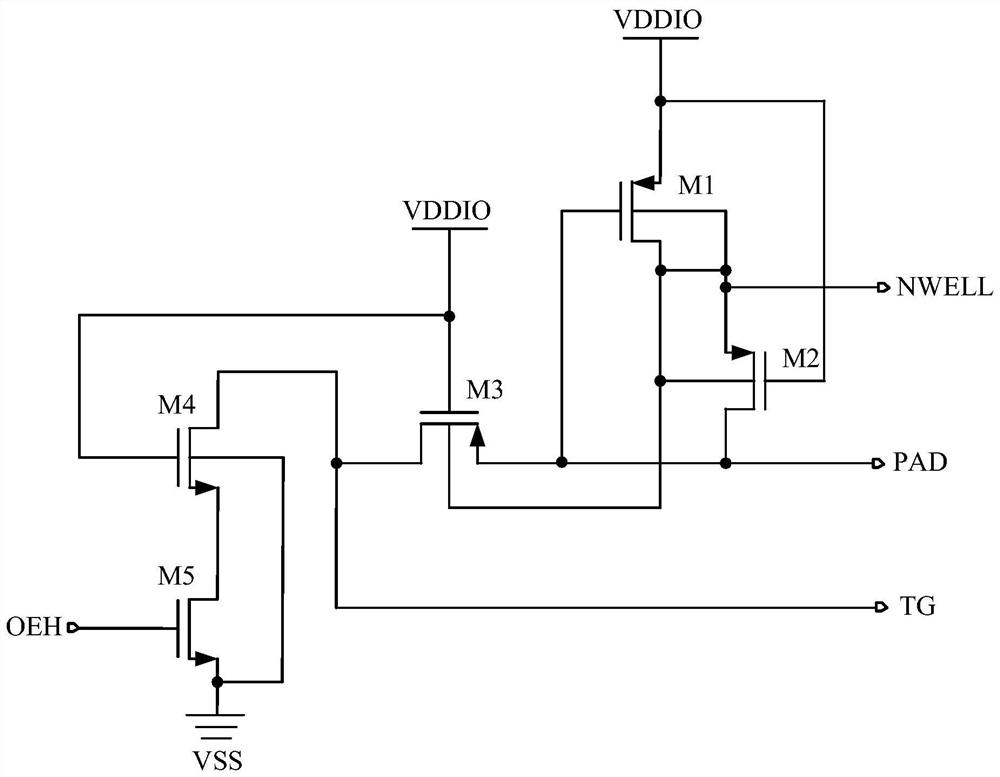
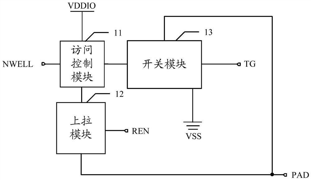
[0030] It will be understood by those skilled in the art that existing pull-up circuits for IO circuits are generally adopted figure 1 The circuit structure shown. in figure 1 In the circuit configuration shown, M1 is an NMOS tube, M2 is a PMOS tube, and the REN is a pull-up control signal, NET1 is a node 1 and is used to connect the source of the NMOS tube M1 and the drain of the PMOS tube M2. according to figure 1 The circuit structure shown is in the failure protection mode (e.g., the voltage value Vddio of the IO power source is suddenly down, and the voltage value of the IO port signal is a logic high), or the input signal voltage value of the IO port is higher than normal. When the voltage value VDDIO of the IO power supply under the work, even if the NMOS tube M1 is turned on, the voltage value of the NET1 is still smaller than the threshold voltage of the IO supply voltage, ensuring that the PAD to IO power from the IO port will not occur. The inverted current appears. How...
PUM
 Abstract
Description
Claims
Application Information


