Surface defect detection device and detection method for high-precision optical element

A technology of optical components and detection devices, which is applied in the field of optical detection, can solve problems such as low detection accuracy, limited practicability, and slow detection speed, and achieve the effects of improving detection efficiency, extending depth of field, and reducing optical resolution.

Inactive Publication Date: 2018-06-12
CHANGGUANG SATELLITE TECH CO LTD
View PDF2 Cites 10 Cited by
  • Summary
  • Abstract
  • Description
  • Claims
  • Application Information

AI Technical Summary

Problems solved by technology

[0004] Based on this, it is necessary to provide a high-precision optical element surface defect detection device and detection method for the problems of

Method used


Image

  • Surface defect detection device and detection method for high-precision optical element
  • Surface defect detection device and detection method for high-precision optical element
  • Surface defect detection device and detection method for high-precision optical element

Examples


Embodiment approach

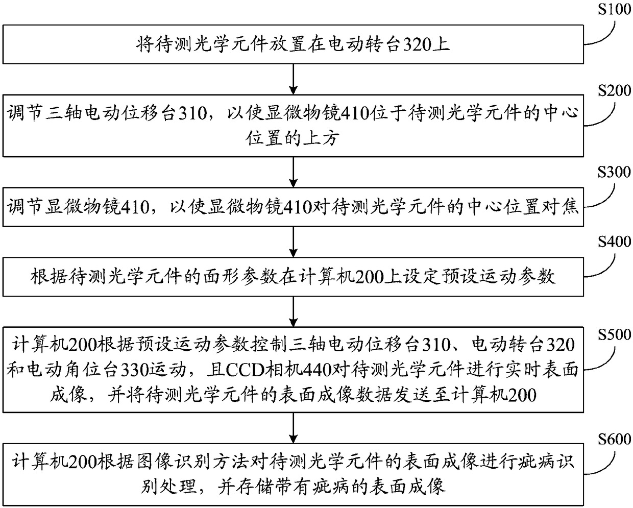
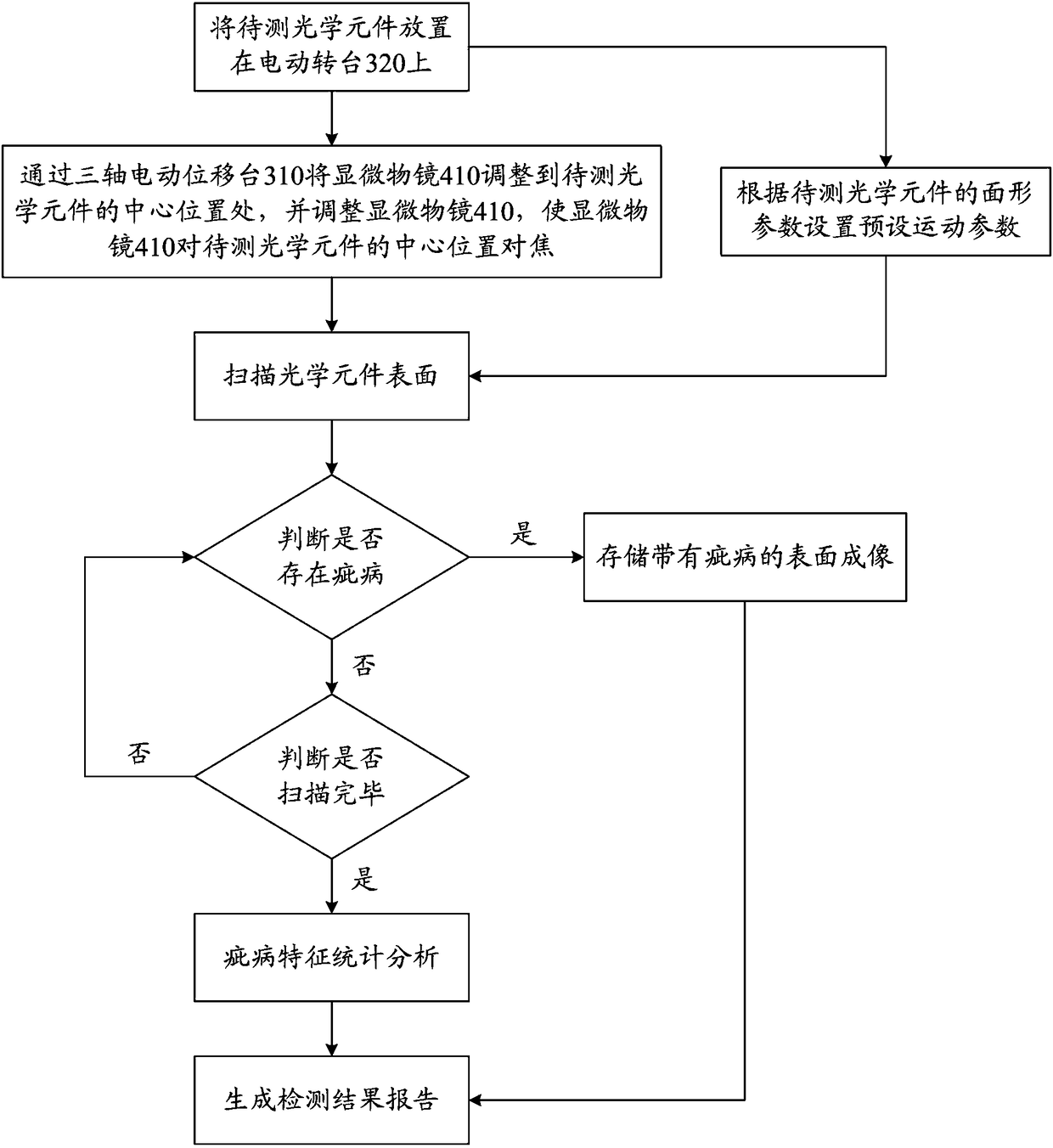
[0056] As a specific implementation, the method for detecting surface defects of high-precision optical components also includes the following steps:

[0057] The computer 200 performs a statistical analysis of defect characteristics on all stored surface images with defects, and generates a test result report, which includes the defect type of the optical element to be tested, the number corresponding to each defect type, and the total number of defects head.

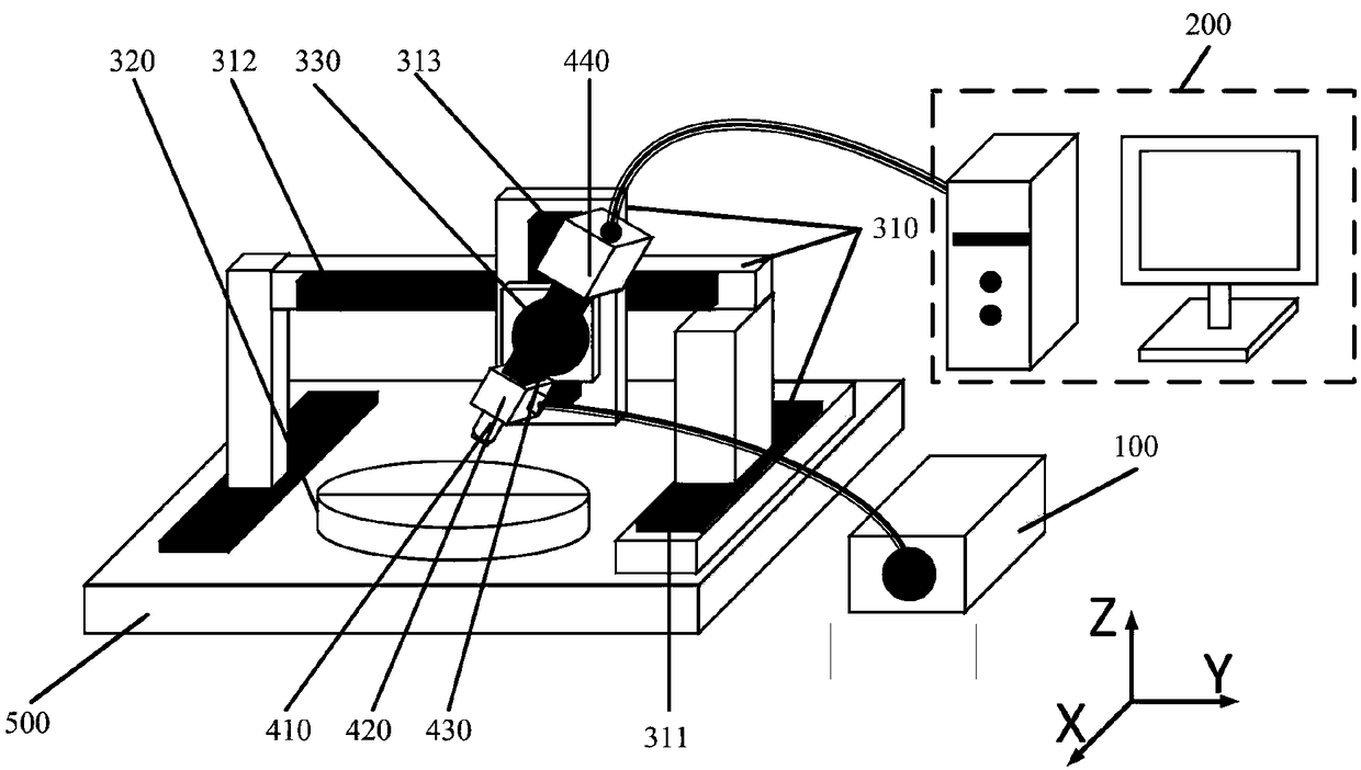
[0058] In this embodiment, if image 3 As shown, the optical element to be tested is placed on the electric turntable 320, and the microscope objective lens 410 is adjusted to the optical position to be tested through the three-axis electric translation stage 310 (mainly through the X-axis electric translation stage 311 and the Y-axis electric translation stage 312). At the center position of the component, adjust the three-axis electric translation stage 310 (mainly the Z-axis electric translation stage 313) and adju...


PUM


Abstract

The invention relates to a surface defect detection device and detection method for a high-precision optical element, and belongs to the technical field of optical detection. The detection device comprises a multiaxial mechanical adjustment module, a wavefront encoding microimaging module, a coaxial light source illumination module and a computer, wherein the multiaxial mechanical adjustment module comprises a triaxial motorized translation stage, a motorized turntablerotation table and a motorized goniometer tablestage; the wavefront encoding microimaging module comprises a microobjective, awavefront encoding plate, a switch lens cone and a CCD (charge-coupled device) camera. According to the surface defect detection device and method for athe high-precision optical element provided by the invention, an imaging effect of an extended depth of field is realized by using the wavefront encoding microimaging module, the depth of field of a general microimaging system is effectively expanded, the defocus caused by a mechanical adjustment error and the surfaces shapes of spherical and non-spherical optical elements is avoided, the requirements on mechanical precision and optical resolution can be lowered, and thus the cost of the surface defect detection device is reduced, and the detection efficiency of the detection device and the detection method is improved.

Description

technical field [0001] The invention relates to the technical field of optical detection, in particular to a surface flaw detection device and detection method for high-precision optical elements. Background technique [0002] Surface defects are an important evaluation index for the surface quality of high-precision optical components. With the continuous development and progress of modern optical technology, optical adaptive astronomical telescopes, large sky area multi-objective spectroscopic astronomical telescopes, lithographic projection objectives, and laser fusion facilities (such as the National Ignition Facility Project of the United States, National Ignition Facility Project, NIF ) and other large optical systems, a large number of high-precision, high-quality spherical and aspheric optical components are used. When the beam passes through the surface of ultra-high-precision optical components with defects, these local structural inhomogeneities cause the scatter...

Claims


Application Information

Patent Timeline
IPC IPC(8): G01N21/95
CPCG01N21/95G01N2021/9511
Inventor 刘江钟兴李艳杰孟瑶苏志强马驰
Owner CHANGGUANG SATELLITE TECH CO LTD
Why Eureka
Try Eureka