Low power consumption compact digital decimation filter for CMOS image sensor

A technology for extracting filters and image sensors, applied in image communication, color TV components, TV system components, etc., can solve the problems of optimizing the number of transistors and power consumption, so as to reduce the number of transistors and facilitate low-cost Effect of low power consumption design and quantity reduction

Active Publication Date: 2018-06-12
重庆湃芯创智微电子有限公司
View PDF7 Cites 5 Cited by
  • Summary
  • Abstract
  • Description
  • Claims
  • Application Information

AI Technical Summary

Problems solved by technology

[0004] Improvements are needed as current conventional digital decimati

Method used


Image

  • Low power consumption compact digital decimation filter for CMOS image sensor
  • Low power consumption compact digital decimation filter for CMOS image sensor
  • Low power consumption compact digital decimation filter for CMOS image sensor

Examples


Embodiment Construction

[0030] The following will be combined with Figure 1-Figure 7 The present invention is described in detail, and the technical solutions in the embodiments of the present invention are clearly and completely described. Apparently, the described embodiments are only some of the embodiments of the present invention, not all of them. Based on the embodiments of the present invention, all other embodiments obtained by persons of ordinary skill in the art without making creative efforts belong to the protection scope of the present invention.

[0031] The present invention provides a kind of low power consumption compact digital decimation filter for CMOS image sensor by improving here, as Figure 2-Figure 7 As shown, it can be implemented as follows;

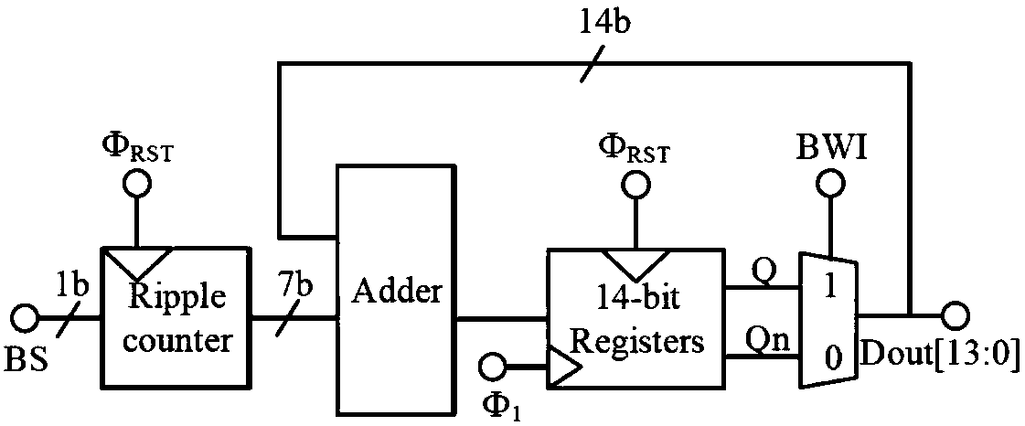
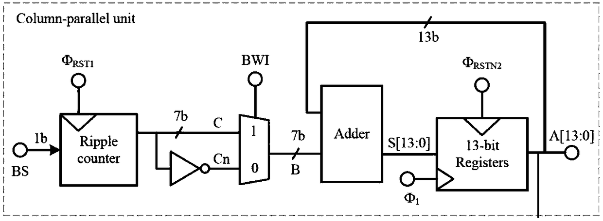
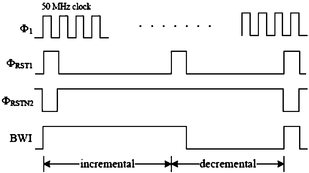
[0032] The overall design of the present invention is as figure 2 As shown, the present invention mainly proposes a special structure, that is, the pre-BWI, which realizes the reduction of the number of transistors and the reducti...


PUM


Abstract

The invention discloses a low power consumption compact digital decimation filter for a CMOS image sensor. The low power consumption compact digital decimation filter comprises a ripple counter, a bit-by-bit inversion module BWI, an adder and a 13-bit register, and an inverter and the bit-by-bit inversion module BWI are arranged in front of the adder, the output data bit width of the ripple counter is 7 bit and is half of the output data bit width of the register; an meanwhile, the register only needs 13 bits to realize a 13-bit dynamic range. In practice, since the output data bit width of the ripple counter is 7 bit and is half of the output data bit width of the register, the number of inverters and selectors is reduced by half compared to the original. Meanwhile, the structure guarantees that the register data will not have the problem of data overflow, so the register only needs 13 bits to realize the 13-bit dynamic range without overflowing the data bit register. The low power consumption compact digital decimation filter disclosed by the invention adopts a special structure of pre-BWI, which greatly reduces the number of filter transistors, reduces the power consumption andreduces the cost.

Description

technical field [0001] The invention relates to the field of integrated circuit design, in particular to a low-power compact digital decimation filter applied in a CMOS image sensor. Background technique [0002] In a traditional column-parallel CMOS image sensor, a combination of a Sigma-Delta modulator and a digital decimation filter is used to realize AD conversion of pixels. Due to the large scale of the pixel array, the modulator and decimation filter will be reused on a large scale. Therefore, the optimization of a single decimation filter will bring about a huge increase in power consumption and area of ​​the entire system. On the premise of ensuring speed and power consumption, the present invention optimizes the number of transistors to improve performance. [0003] Such as figure 1 Shown is a traditional second-order digital decimation filter structure, which is essentially formed by cascading two-stage digital integrators. The first-stage digital integrator is a...

Claims


Application Information

Patent Timeline
IPC IPC(8): H04N5/374H04N5/3745H04N5/378
CPCH04N25/767H04N25/76H04N25/77H04N25/75
Inventor 唐枋
Owner 重庆湃芯创智微电子有限公司
Why Eureka
Try Eureka