Chip thinning-based cleaning method

A chip and LED chip technology, applied in the field of cleaning, can solve the problem of unclean silicon substrate cleaning, and achieve the effect of environmental protection

Inactive Publication Date: 2018-06-15
南昌易美光电科技有限公司
View PDF9 Cites 2 Cited by
  • Summary
  • Abstract
  • Description
  • Claims
  • Application Information

AI Technical Summary

Problems solved by technology

[0005] The purpose of the present invention is to provide a cleaning method based on chip thinning, which effectively solves the technical problem in the prior art that the silicon substrate is not clean after thinning

Method used


Image

  • Chip thinning-based cleaning method

Examples


Embodiment Construction

[0022] The essence of the present invention will be further described below in conjunction with the accompanying drawings and examples, but the content of the present invention is not limited thereto.

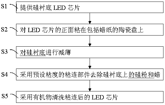
[0023] like figure 1 Shown is a schematic flow chart of the cleaning method based on chip thinning provided by the present invention. It can be seen from the figure that the cleaning method includes:

[0024] S1 provides silicon substrate LED chips;

[0025] S2 The front side of the LED chip is glued to the ceramic plate including the wax paper;

[0026] S3 Thinning the silicon substrate;

[0027] S4 removes the silicon powder and wax on the silicon substrate by using an adhesive part with a preset viscosity;

[0028] S5 Use organic matter to clean the bonded LED chips.

[0029] In this cleaning method, the adhesive part selected is preferably an adhesive film, such as the blue film widely used in laboratories at present, and the viscosity range is selected between 0.5 and ...


PUM


Abstract

The invention discloses a chip thinning-based cleaning method. The chip thinning-based cleaning method comprises the steps of providing a silicon substrate LED chip; pasting a front surface of the LEDchip onto a ceramic disc comprising wax paper; thinning the silicon substrate; removing silicon powder and wax on the silicon substrate by employing a pasting part with preset viscosity; and cleaningthe pasted LED chip with an organic substance. Before cleaning the LED chip with a cleaning liquid, the silicon powder and the wax are removed by a physical mode, the electrical characteristic of theLED chip cannot be affected, and environmental protection is facilitated.

Description

technical field [0001] The invention relates to the technical field of semiconductors, in particular to a cleaning method. Background technique [0002] In the process of chip preparation, the growth substrate usually needs to be thinned, and it needs to be cleaned after thinning. If the cleaning is not clean, the quality of the chip will be directly affected. [0003] At present, in the process of thinning the silicon substrate, the front of the chip is generally stuck to a ceramic disc with wax paper, and the back of the substrate is ground and thinned with a grinder, and then the chip is removed for cleaning. During the cleaning process, the residual wax and silicon powder are first cleaned with a dewaxing solution, then ultrasonically cleaned with organic matter, and finally the metal is steamed on the back. However, this cleaning method still has the phenomenon of unclean cleaning, which leads to serious peeling off of the back gold of the chip; in addition, ultrasonic...

Claims


Application Information

Patent Timeline
Patent Type & Authority Applications(China)
IPC IPC(8): H01L21/02H01L21/67
Inventor 王丽
Owner 南昌易美光电科技有限公司
Why Eureka
Try Eureka