Adsorption method of warped wafer and device using the adsorption method

A wafer and warping technology, applied in the manufacturing of electrical components, circuits, semiconductor/solid-state devices, etc., can solve problems such as affecting productivity, reducing wafer warpage, and inability of wafer to be adsorbed, so as to reduce costs, The effect of improving the yield

Active Publication Date: 2021-02-02
DYNAX SEMICON
View PDF5 Cites 0 Cited by
  • Summary
  • Abstract
  • Description
  • Claims
  • Application Information

AI Technical Summary

Problems solved by technology

There are usually multiple suction holes on the suction cup to better fix the wafer. When the wafer is flat or only slightly warped, the suction cup can absorb the wafer and reduce the warpage of the wafer; but when the wafer When the deformation is serious, there will be a vacuum leak between the chuck and the wafer, which will cause the wafer to be unable to be adsorbed, resulting in rejection of the wafer, which greatly affects the yield

Method used


Image

  • Adsorption method of warped wafer and device using the adsorption method
  • Adsorption method of warped wafer and device using the adsorption method
  • Adsorption method of warped wafer and device using the adsorption method

Examples


Embodiment Construction

[0035] The technical solutions of the present invention will be further described below in conjunction with the accompanying drawings and through specific implementation methods.

[0036] Preferred embodiment:

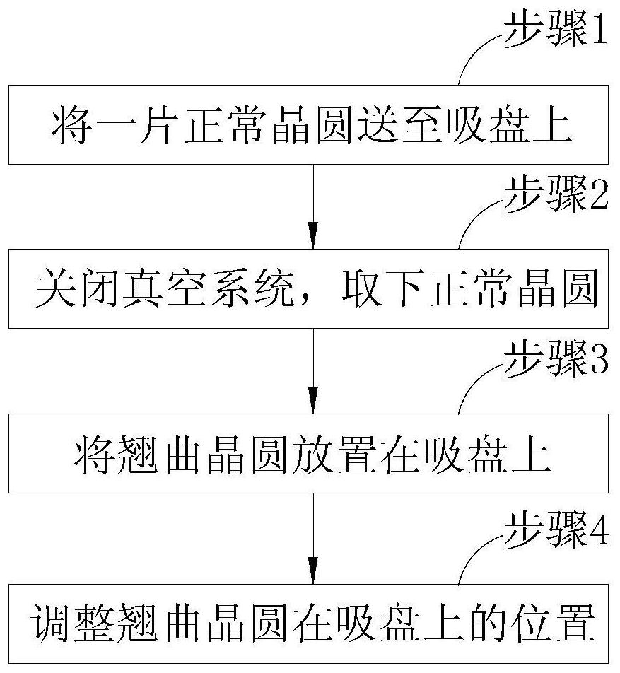
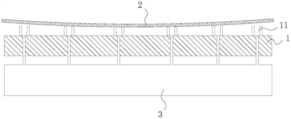
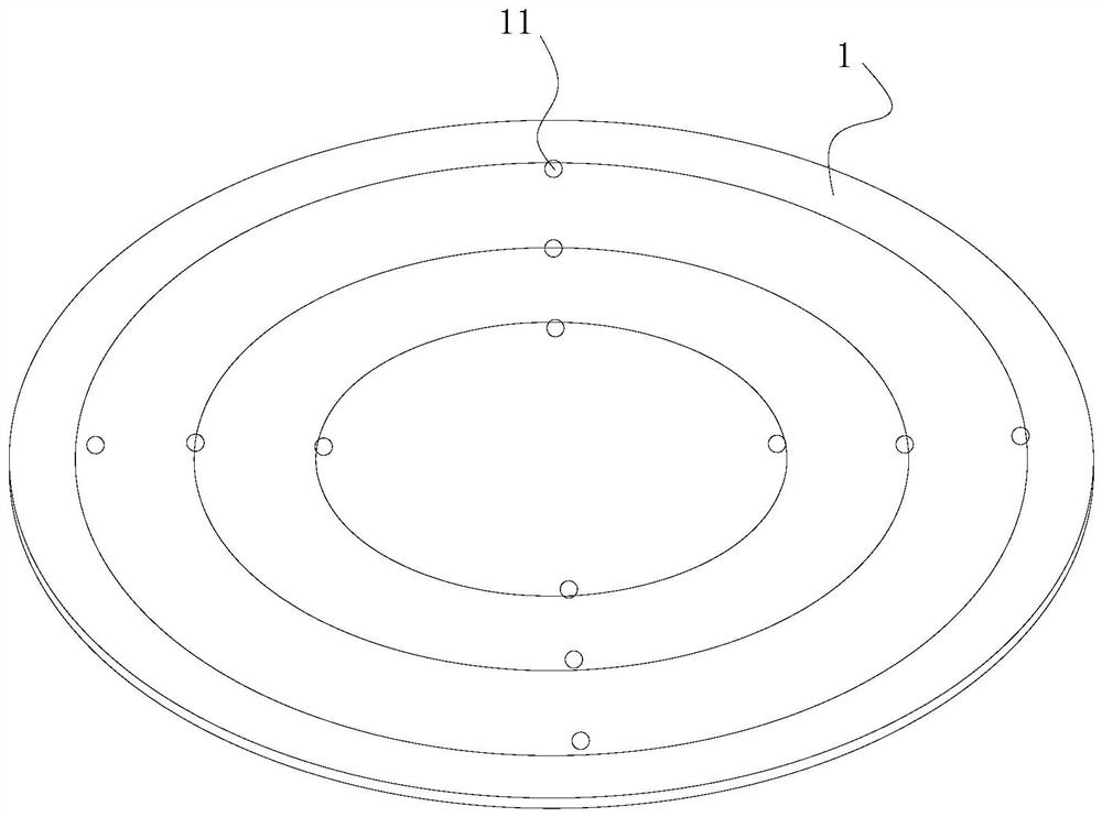
[0037] This preferred embodiment discloses an adsorption method for a warped wafer. The adsorption method is to use a normal wafer to form a normal adsorption state on the chuck 1, then use a warped wafer 2 to replace the normal wafer, and adjust the position of the warped wafer 2 on the chuck 1 horizontally and / or rotate until it is warped. The curved wafer 2 is adsorbed on the chuck 1 .

[0038] The production and processing of semiconductor wafers takes a relatively long time, especially those wafers with more complicated processing procedures. At the final stage of the entire processing (such as engraving metal wiring or pressing points), it is found that some products cannot be processed due to warping and deformation. Re-introduction of a certain amount of prod...


PUM


Abstract

The invention discloses an adsorption method for a warped wafer and a device using the adsorption method, which belong to the technical field of semiconductors and are designed to solve the problem that the existing warped wafer cannot be adsorbed. The adsorption method of the warped wafer in the present invention is to use a normal wafer to form a normal state of adsorption on the chuck, then use the warped wafer to replace the normal wafer, and adjust the position of the warped wafer on the chuck by horizontal adjustment and / or rotation until the warped wafer is absorbed on the chuck. The device of the invention comprises a suction cup connected to a vacuum system, and a plurality of suction holes are arranged on the suction cup; a control switch is arranged on the vacuum system. The adsorption method of the warped wafer of the present invention avoids discarding the wafer due to warping as much as possible, so that as many wafers as possible can be successfully cut into chips, the yield rate is improved, and the cost is reduced. The device of the present invention can use the above-mentioned adsorption method to photoetch warped wafers, avoiding these wafers from being discarded, and the photoetching effect is good.

Description

technical field [0001] The invention relates to the technical field of semiconductors, in particular to an adsorption method for a warped wafer and a device using the adsorption method. Background technique [0002] In the semiconductor manufacturing process, a large amount of stress will inevitably accumulate on the wafer after going through multiple processes, resulting in partial or total warping of the wafer, and even when the stress exceeds the limit that the wafer can withstand resulting in chipping of the wafer. [0003] The exposure process needs to place the wafer on the suction cup, absorb and fix it through the vacuum suction hole on the suction cup, and then perform photolithography on the wafer. There are usually multiple suction holes on the suction cup to better fix the wafer. When the wafer is flat or only slightly warped, the suction cup can absorb the wafer and reduce the warpage of the wafer; but when the wafer When the deformation is severe, a vacuum le...

Claims


Application Information

Patent Timeline
Patent Type & Authority Patents(China)
IPC IPC(8): H01L21/67H01L21/683
CPCH01L21/67259H01L21/67271H01L21/6838
Inventor 陈明辉
Owner DYNAX SEMICON
Why Eureka
Try Eureka