
Eureka
For R&D, Eureka makes reading and utilizing patents & technical documents easy.
Eureka AIR
Designed for self-driven R&D workflows. Generate viable solutions, solve complex R&D challenges, empower your innovation with AI.

Eureka Materials
Designed for material experts only. Revolutionize your material R&D, from search, analyze, to developing new materials.

TechResearch
Generate reliable direction feasibility study reports for your R&D in just a few steps.

TechSeek
Discover and master advanced knowledge NOW. Basics, ideas, possibilities, all at once.

TechMind
As an expert in R&D Theories, TechMind can generates customized viable solutions instantly.

TechRisk
Analyze your overall solution with one click, know your potential R&D risks in advance.

TechMonitor
Get weekly tech updates, stay abreast of the latest tech innovations and key insights.
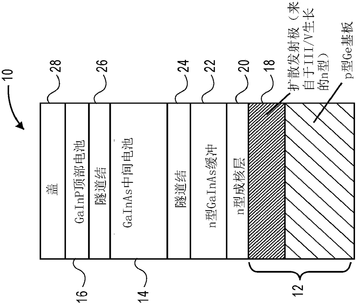
Multijunction solar cell having patterned emitter and method of making the solar cell
A technology of solar cells and solar sub-cells, applied in photovoltaic power generation, circuits, electrical components, etc., can solve problems such as reducing the efficiency of solar cells
- Summary
- Abstract
- Description
- Claims
- Application Information
AI Technical Summary
Problems solved by technology
Method used
Image

Examples
Embodiment 1
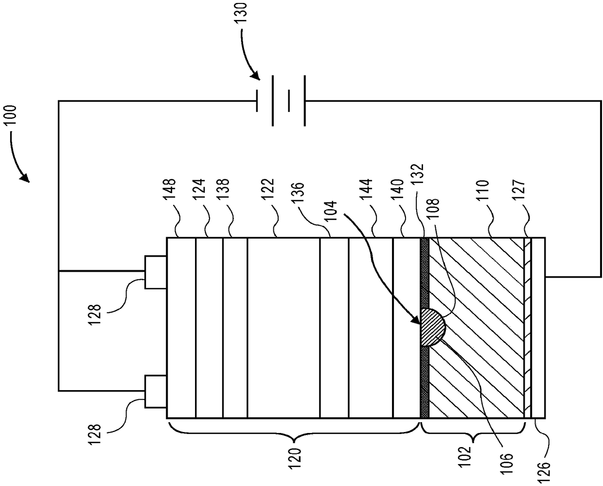
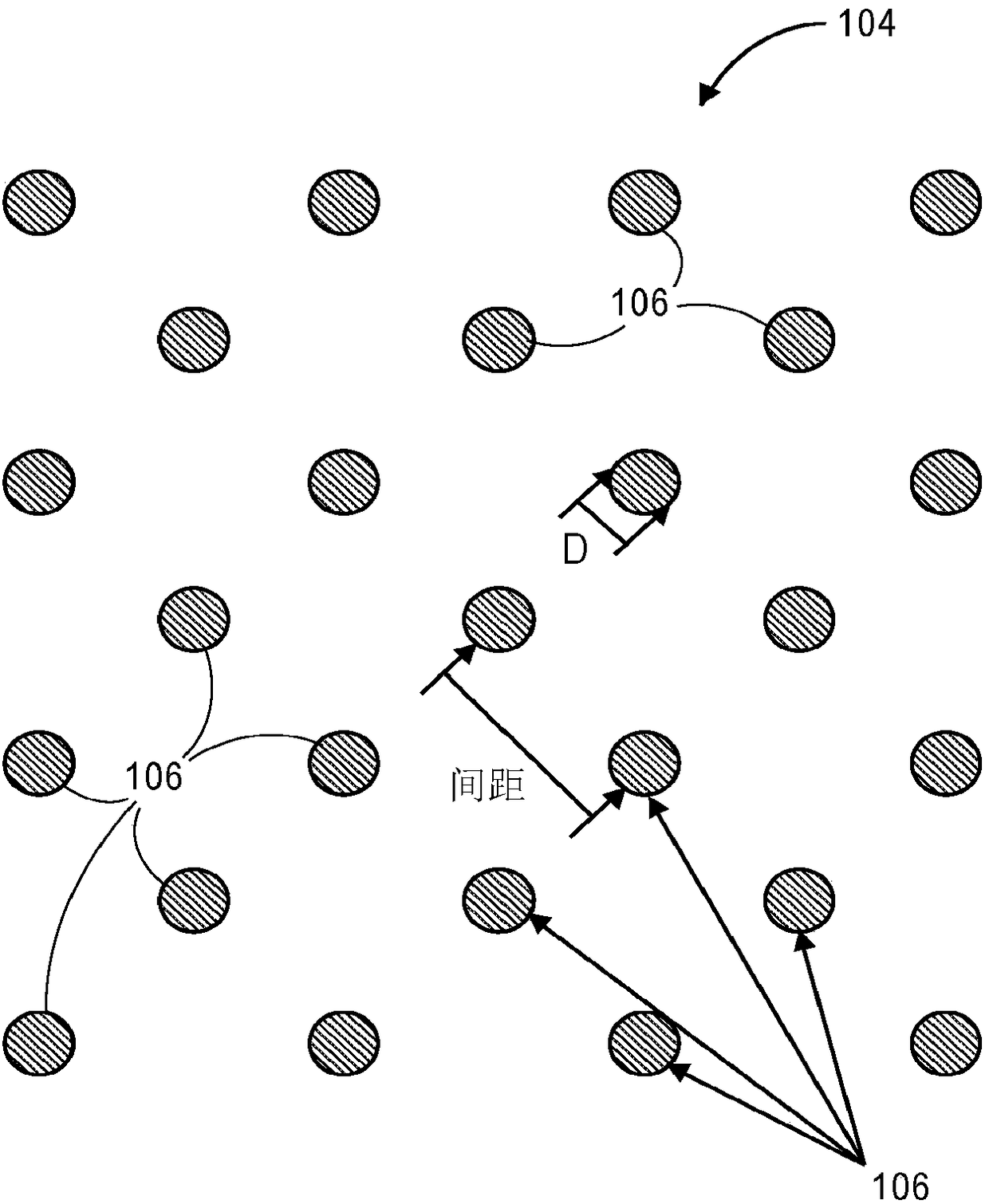
[0054] Embodiment 1. A multi-junction solar cell comprising: a base substrate comprising a Group IV semiconductor and a dopant of a first carrier type; a patterned emitter formed at a first surface of the base substrate, The patterned emitter includes a plurality of well regions doped with a dopant of the second carrier type in the Group IV semiconductor, the base substrate includes the patterned emitter forming the first solar subcell; and the upper structure includes One or more additional solar subcells above the first solar subcell.
Embodiment 2
[0055] Embodiment 2. The multi-junction solar cell of embodiment 1, further comprising a passivation layer at the first surface of the base substrate positioned between the patterned emitter well regions and comprising a second A carrier type dopant.
Embodiment 3
[0056] Embodiment 3. The multijunction solar cell of embodiment 1 or 2, wherein the Group IV semiconductor comprises a material selected from germanium and silicon.
PUM
 Abstract
Description
Claims
Application Information
 - R&D Engineer
- R&D Manager
- IP Professional
- Industry Leading Data Capabilities
- Powerful AI technology
- Patent DNA Extraction
Browse by: Latest US Patents, China's latest patents, Technical Efficacy Thesaurus, Application Domain, Technology Topic, Popular Technical Reports.
© 2024 PatSnap. All rights reserved.Legal|Privacy policy|Modern Slavery Act Transparency Statement|Sitemap|About US| Contact US: help@patsnap.com