SRAM read and write indirect testing device and method based on LabVIEW
A test device and indirect technology, applied in static memory, instruments, etc., can solve the problems of inflexible control configuration of direct reading and writing SRAM, unfriendly test interface, etc., and achieve simple test interface, simple and convenient timing adjustment, and intuitive interface Effect
- Summary
- Abstract
- Description
- Claims
- Application Information
AI Technical Summary
Problems solved by technology
Method used
Image
Examples
Embodiment Construction
[0021] Below in conjunction with accompanying drawing, the present invention is described in further detail:
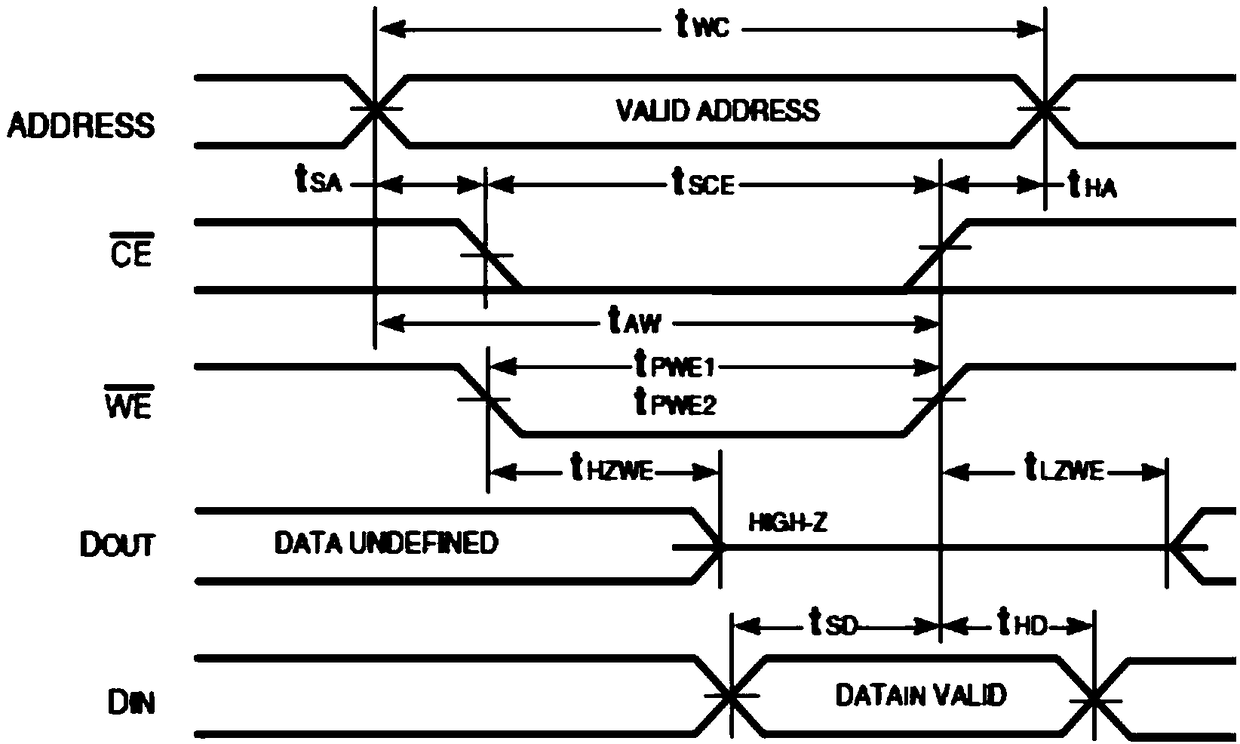
[0022] like figure 1 Shown is the IS61LV10248 chip write operation timing diagram, in which:
[0023] t WC Indicates Write Cycle Time;
[0024] t SCE Indicates CE to Write End;
[0025] t AW Indicates Address Setup Time to Write End;
[0026] t HA Indicates Address Hold from Write End;
[0027] t SA Indicates Address Setup Time;
[0028] t PWE1 Indicates WE Pulse Width;
[0029] t PWE2 Indicates WE Pulse Width (OE=LOW);
[0030] t SD Indicates Data Setup to Write End;
[0031] t HD Indicates Data Hold from Write End;
[0032] t HZWE Indicates WE LOW to High-Z Output;
[0033] t LZWE Indicates WE HIGH to Low-Z Output.
[0034] Depend on figure 1 It can be known that the IS61LV10248 chip is valid for writing data, it must satisfy the chip select signal CE / , and the write enable WE / is low; at the same time, it must satisfy the address signal ADRESS...
PUM
 Abstract
Description
Claims
Application Information


