Display panel manufacturing method, display panel, and display device

A manufacturing method and technology for display panels, which are applied in the fields of semiconductor/solid-state device manufacturing, electrical components, circuits, etc., can solve problems such as disadvantage and productivity, pattern shift, high production cost, etc.

Active Publication Date: 2018-07-10
BOE TECH GRP CO LTD +1
View PDF14 Cites 4 Cited by
  • Summary
  • Abstract
  • Description
  • Claims
  • Application Information

AI Technical Summary

Problems solved by technology

For TFT-LCD, the thin film manufacturing process needs to use a large number of masks, and the mold of the mask has a high production cost, which is not conducive to improving production efficiency.
On the other hand, it is necessary to precisely align the composition position when using a mask to form a pattern, otherwise many defects will occur due to pattern offset, and there is a certain limit for the control of pattern alignment in the prior art, so Unable to effectively avoid the offset problem of graphics

Method used


Image

  • Display panel manufacturing method, display panel, and display device
  • Display panel manufacturing method, display panel, and display device
  • Display panel manufacturing method, display panel, and display device

Examples


Embodiment Construction

[0045] In view of the problems in the prior art, the embodiments of the present invention provide a method for manufacturing a display panel, a display panel, and a display device, which are used to eliminate the problem of graphic offset in the manufacturing process.

[0046] In the following, with reference to the accompanying drawings, the manufacturing method of the display panel, the display panel and the display device provided by the embodiments of the present invention will be described in detail. Wherein, the thickness and shape of each component in the drawings do not reflect the true proportions of the display panel or the display device, and are only intended to illustrate the content of the present invention.

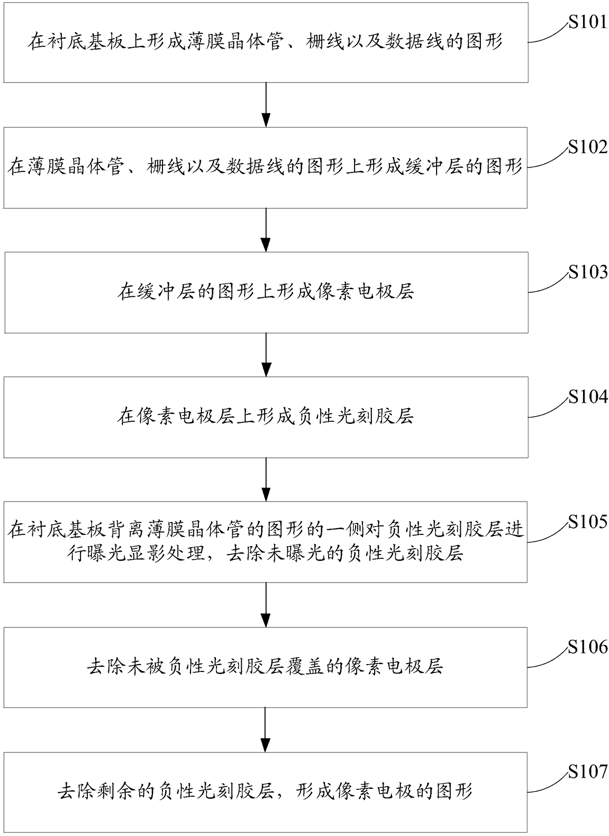
[0047] Such as figure 1 As shown, the manufacturing method of the display panel provided by the embodiment of the present invention may include the following steps:

[0048] S101, forming patterns of thin film transistors, gate lines and data lines on a base subst...


PUM


Abstract

The invention discloses a display panel manufacturing method, a display panel, and a display device. The method comprises the steps: forming a thin film transistor pattern, a grid line pattern and a data line pattern on a substrate, wherein the thin film transistor pattern comprises a connecting block connected with the drain electrode of a thin film transistor, and the connecting block is provided with a plurality of hollow-out structures; carrying out the exposing and developing processing of a negative photoresist layer at one side, backing on to the thin film transistor, of the substrate,and removing the non-exposed part of the negative photoresist layer; removing a pixel electrode layer which is not covered by the negative photoresist layer; removing the remaining negative photoresist layer, and forming a pixel electrode pattern. The thin film transistor pattern, the grid line pattern and the data line pattern are taken as the mask templates, and the pixel electrode pattern is formed in an autocollimation mode, thereby avoiding a collimation problem caused by the application of a mask, and causing no pattern offset. Meanwhile, the method saves the mask which is used for manufacturing a pixel electrode, thereby saving the production cost.

Description

Technical field [0001] The present invention relates to the field of display technology, in particular to a manufacturing method of a display panel, a display panel and a display device. Background technique [0002] Thin Film Transistor-Liquid Crystal Display (TFT-LCD) has the characteristics of small size, low power consumption, and no radiation, and it occupies a dominant position in the current flat panel display market. For the TFT-LCD, a large number of masks are required to adopt a thin film manufacturing process, and the mold of the mask has a high production cost, which is not conducive to improving and yielding efficiency. On the other hand, it is necessary to precisely align the composition position when using a mask to compose a picture. Otherwise, a lot of defects will occur due to the pattern shift. The prior art has a certain limit on the control of pattern alignment. Can not effectively avoid the problem of graphic offset. Summary of the invention [0003] Embodi...

Claims


Application Information

Patent Timeline
Patent Type & Authority Applications(China)
IPC IPC(8): H01L21/84
CPCH01L21/84
Inventor 王兆君黄中浩高坤坤张超田茂坤杨宇桐吴旭
Owner BOE TECH GRP CO LTD
Why Eureka
Try Eureka