LED (light-emitting diode) chip and preparation method thereof

A technology of LED chip and epitaxial layer, which is applied in the direction of electrical components, circuits, semiconductor devices, etc., can solve the problems of poor adhesion of N-type epitaxial layer, reduce luminous intensity and efficiency, and affect the firmness of wafer bonding, etc., to achieve Not easy to peel off, improve luminous intensity and efficiency, low cost effect

Inactive Publication Date: 2018-07-13
ENRAYTEK OPTOELECTRONICS
View PDF3 Cites 0 Cited by
  • Summary
  • Abstract
  • Description
  • Claims
  • Application Information

AI Technical Summary

Problems solved by technology

[0003] However, in the vertical structure of the LED chip, the area under the N electrode is the most concentrated area of ​​current injection, and this part of the light will be blocked or absorbed by the electrode and eventually become invalid light, thereby reducing the luminous intensity and efficiency of the LED.
At present, in order to solve this problem, a current blocking layer is often introduced into the vertical structure LED chip to limit or greatly reduce the light emission of the active layer under the N electrode, such as commonly used SiO 2 or Si 3 N 4 As current blocking layer materials, however, the preparation process of these materials is complicated and the cost is high; and these materials have the problem of poor adhesion to the N-type epitaxial layer, which seriously affects the firmness of wafer bonding, resulting in poor substrate peeling. rate degrades and affects the reliability of the LED

Method used


Image

  • LED (light-emitting diode) chip and preparation method thereof
  • LED (light-emitting diode) chip and preparation method thereof
  • LED (light-emitting diode) chip and preparation method thereof

Examples


preparation example Construction
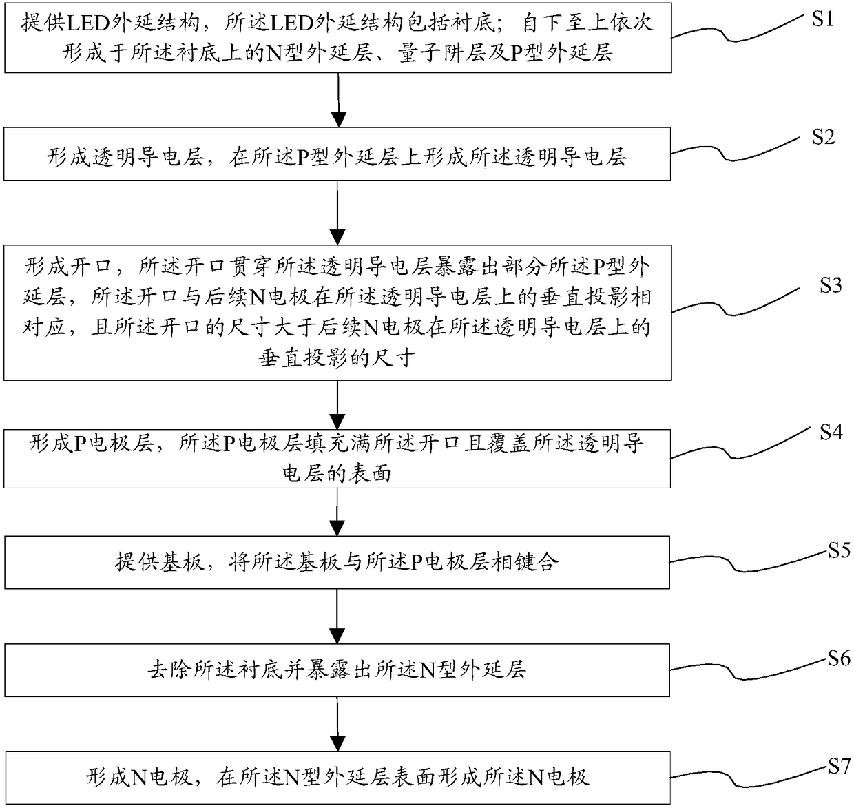
[0040] The core idea of ​​the present invention is that the present invention provides a method for preparing an LED chip, such as figure 1 Shown, described preparation method comprises the following steps:

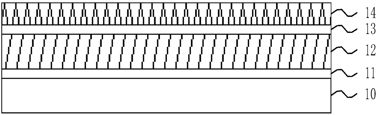
[0041] Step S1, providing an LED epitaxial structure, the LED epitaxial structure includes a substrate; an N-type epitaxial layer, a quantum well layer, and a P-type epitaxial layer are sequentially formed on the substrate from bottom to top;

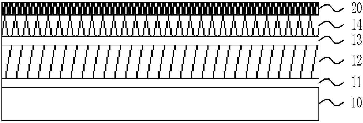
[0042] Step S2, forming a transparent conductive layer, forming the transparent conductive layer on the P-type epitaxial layer;

[0043] Step S3, forming an opening, the opening penetrates through the transparent conductive layer to expose part of the P-type epitaxial layer, the opening corresponds to the vertical projection of the subsequent N electrode on the transparent conductive layer, and the opening The size is larger than the size of the vertical projection of the subsequent N electrode on the transparent conductive layer;...


PUM


Abstract

The invention discloses an LED (light-emitting diode) chip and a preparation method thereof. The preparation method includes the steps: forming a transparent conductive layer on a P-type epitaxial layer of an LED epitaxial structure; forming an opening penetrating the transparent conductive layer and exposing part of the P-type epitaxial layer; forming a P electrode layer filling the opening and covering the surface of the transparent conductive layer; forming an N electrode on the surface of an N-type epitaxial layer. The opening corresponds to the vertical projection of the N electrode on the transparent conductive layer, and the size of the opening is larger than that of the vertical projection of the N electrode on the transparent conductive layer. The P-type epitaxial layer exposed tothe opening directly contacts with the P electrode layer, a current blocking structure is formed in a high-contact resistance area between the P-type epitaxial layer and the P electrode layer, injection current is effectively extended, crowding of current below the N electrode is relieved, and uniform distribution of the current is improved, so that the luminous intensity and efficiency of the LED chip are improved.

Description

technical field [0001] The invention belongs to the field of semiconductor light emitting, in particular to an LED chip and a preparation method thereof. Background technique [0002] With the continuous development of light-emitting diode (Light Emitting Diode, referred to as LED) technology, LED chips have traditional front-mounted structures, flip-chip structures, and vertical structures. Because vertical-structured LED chips have good heat dissipation, can carry large currents, and have high luminous intensity , low power consumption, long life and other advantages, are widely used in general lighting, landscape lighting, special lighting, automotive lighting and other fields. [0003] However, in a vertically structured LED chip, the area under the N electrode is where the current injection is most concentrated, and this part of the light will be blocked or absorbed by the electrode and eventually become ineffective light emission, thereby reducing the luminous intensit...

Claims


Application Information

Patent Timeline
IPC IPC(8): H01L33/00H01L33/14H01L33/22H01L33/36
CPCH01L33/005H01L33/145H01L33/22H01L33/36
Inventor 童玲
Owner ENRAYTEK OPTOELECTRONICS
Why Eureka
Try Eureka