A method for measuring the coplanarity of solder balls in BGA packaged chips

A technology of coplanarity and chip mounting, applied in the field of measurement, can solve the problems in the field of measurement of coplanarity of solder balls that are not applied, and achieve the effects of high dynamic measurement accuracy, easy follow-up development, and good anti-interference performance.

Active Publication Date: 2019-12-10
TIANJIN JINHANG COMP TECH RES INST
View PDF5 Cites 0 Cited by
  • Summary
  • Abstract
  • Description
  • Claims
  • Application Information

AI Technical Summary

Problems solved by technology

However, this measurement method has not been applied to the field of solder ball coplanarity measurement

Method used


Image

  • A method for measuring the coplanarity of solder balls in BGA packaged chips

Examples


Embodiment Construction

[0024] Specific examples of the present invention are given below. The specific embodiments are only used to further describe the present invention in detail, and do not limit the protection scope of the claims of the present application.

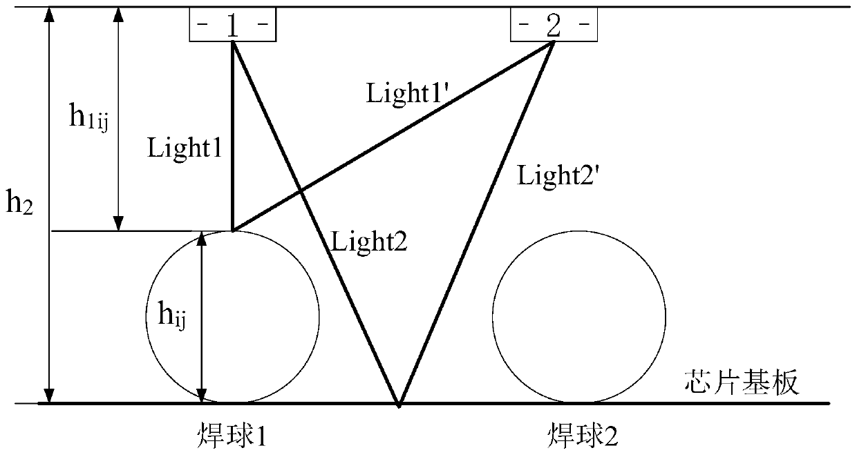
[0025] The invention provides a method for measuring the coplanarity of solder balls of BGA packaged chips. In the method, a gamma photon source 1 equipped with a collimator is used to irradiate a BGA packaged chip in a safe environment, and the gamma photon interacts with the chip and is reflected to a receiving processor 2 . The scintillator in the receiving processor 2 receives the photons backscattered by the chip and multiplies them through the photomultiplier tube to obtain the photon counting frequency by the processing circuit. After simulation, the height from the top surface of the solder ball to the receiving processor is obtained, and then the height of the solder ball is obtained. .

[0026] The method for measuring the copla...


PUM


Abstract

The invention discloses a method for measuring the coplanarity of the solder balls of a BGA (Ball Grid Array) packaged chip. A gamma photon source equipped with a collimator is used to radiate a BGA packaged chip in a secure environment, and the gamma photons are reflected to a receiving processor after reacting with the chip. A scintillator in the receiving processor receives the photons backscattered by the chip. After a photomultiplier multiplies the photons, a processing circuit obtains the photon counting frequency. The height from the top of the solder balls to the receiving processor isobtained by simulation, and then, the height of the solder balls is obtained.

Description

technical field [0001] The invention relates to the field of measurement, in particular to a method for measuring the coplanarity of solder balls of BGA packaged chips. Background technique [0002] Pin coplanarity is one of the most important indicators for detecting whether a device is qualified. Although during surface mounting, the reflowed solder balls and solder paste will re-melt to form solder joints to realize the connection between the chip and the chip substrate, thereby overcoming the coplanarity problem caused by solder balls of different heights, but if the device The coplanarity of the solder ball pins exceeds the standard, and individual solder balls are in poor contact with the board during installation, which will lead to missed connections and virtual connections. [0003] Since the packaged device is installed on the board, the solder joints of the pins are hidden at the bottom of the chip, it is difficult to detect the quality of the solder joints by di...

Claims


Application Information

Patent Timeline
IPC IPC(8): G01B15/00
CPCG01B15/00
Inventor 张楠朱天成李鑫候俊马王旭仇旭东
Owner TIANJIN JINHANG COMP TECH RES INST
Why Eureka
Try Eureka