Unlock instant, AI-driven research and patent intelligence for your innovation.

A CMOS high temperature reference voltage source

A reference voltage source and MOS tube technology, applied in the direction of adjusting electrical variables, instruments, control/regulation systems, etc., can solve problems such as BJT failure and low efficiency, and achieve high power supply noise suppression, low output noise, and low operating temperature coefficient Effect

Active Publication Date: 2020-10-02
HANGZHOU T ADC MICROELECTRONICS CO LTD
View PDF2 Cites 0 Cited by
  • Summary
  • Abstract
  • Description
  • Claims
  • Application Information

AI Technical Summary

Problems solved by technology

When the temperature is higher than 150℃, BJT is very likely to fail due to leakage and extremely inefficient emitter

Method used


Image

  • A CMOS high temperature reference voltage source
  • A CMOS high temperature reference voltage source
  • A CMOS high temperature reference voltage source

Examples


Embodiment Construction

[0047] The technical solutions of the present invention will be described in further detail below with reference to the accompanying drawings and embodiments.

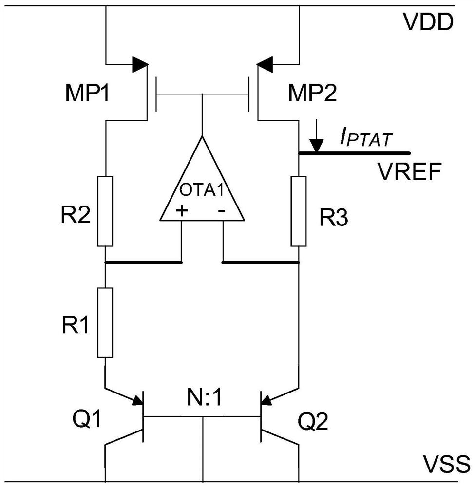
[0048] image 3 It is a schematic diagram of a CMOS high-temperature reference voltage source circuit realized according to an embodiment of the present invention.

[0049] Such as image 3As shown, the CMOS high-temperature reference circuit includes a start-up circuit and a bias circuit for properly biasing the reference core circuit. Wherein, the start-up circuit is used to start the bias circuit, so that when the circuit is powered on, it can drive the circuit to get rid of the degenerate bias point, start normally and work stably, and prevent the bias circuit from operating at the bias current IB=0. state.

[0050] In one embodiment, the start-up circuit includes PMOS transistor P1, PMOS transistor P2 and three NMOS transistors N1, N2, N3. The three NMOS transistors are connected sequentially, the source of N1 ...


PUM


Abstract

A CMOS high temperature reference voltage source, comprising: a reference core circuit, specifically comprising: a first PMOS tube M4, a low voltage difference linear stabilizer LDO, and a first impedance circuit and a second impedance circuit in serial connection to each other; also comprised are: a third resistor R3, a fourth resistor R4, and a third impedance circuit and fourth impedance circuit in serial connection to each other; by means of the reference core circuit, a reference voltage architecture of a MOSFET and resistors are combined using binary weighting, so as to achieve a low temperature coefficient voltage reference which has a wide expansion range up to 230℃, and the architecture has high power source noise suppression, low output noise and a low operating temperature coefficient, such as -40℃-230℃, in simulations.

Description

technical field [0001] The invention relates to a CMOS voltage source, in particular to a CMOS high-temperature reference voltage source. Background technique [0002] Traditionally, the CMOS silicon bulk process can be widely used in the temperature range of -40°C to 150°C. When the additional higher voltage will cause abnormal operation of those small bandgap devices, such as silicon bulk bandgap voltage = 1.12eV. In order to meet the use above 150°C, people choose other higher bandgap processes, such as SiGe (bandgap = 3.2eV). In standard CMOS processes (including bulk silicon or SOI), there are few solutions for the design target of 150°C or higher, especially for those BJT-based bandgap voltage references. When the temperature is higher than 150°C, the BJT is very likely to fail due to leakage and extremely inefficient emitters. Therefore, for analog-to-digital converters ADCs and digital-to-analog converters DACs, it is essential to implement high-temperature voltag...

Claims


Application Information

Patent Timeline
Patent Type & Authority Patents(China)
IPC IPC(8): G05F3/26
CPCG05F3/26G05F3/245G05F3/30
Inventor 陈乐峰陆文正
Owner HANGZHOU T ADC MICROELECTRONICS CO LTD