Wafer defect searching system and wafer defect searching method

A defect and wafer technology, applied in the field of wafer defect search and wafer defect search system, can solve problems such as inability to take pictures in real time, difficulty in finding wafer defects, etc., to achieve great significance, improve yield, and improve circulation speed Effect

Inactive Publication Date: 2018-07-24
SHANGHAI HUALI MICROELECTRONICS CORP
View PDF5 Cites 9 Cited by
  • Summary
  • Abstract
  • Description
  • Claims
  • Application Information

AI Technical Summary

Problems solved by technology

[0005] The purpose of the present invention is to provide a new method for finding wafer defects, so as to solv

Method used


Image

  • Wafer defect searching system and wafer defect searching method
  • Wafer defect searching system and wafer defect searching method
  • Wafer defect searching system and wafer defect searching method

Examples


Embodiment Construction

[0023] The specific implementation manner of the present invention will be described in more detail below with reference to schematic diagrams. Advantages and features of the present invention will be apparent from the following description and claims. It should be noted that all the drawings are in a very simplified form and use imprecise scales, and are only used to facilitate and clearly assist the purpose of illustrating the embodiments of the present invention.

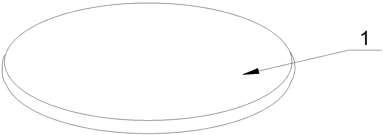
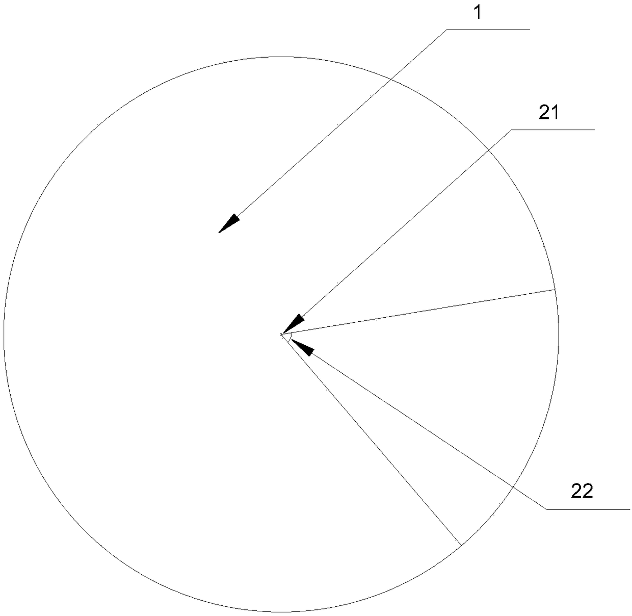
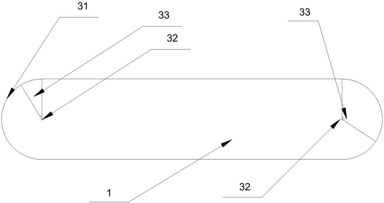
[0024] Please refer to figure 1 , figure 2 with image 3 , figure 1 Wafer structure diagram provided for the embodiment of the present invention; figure 2 Provided for the embodiment of the present invention figure 1 top view of image 3 Provided for the embodiment of the present invention figure 1 side sectional view.

[0025] The present invention provides a method for finding defects on a wafer 1 to solve the problems in the prior art that it is difficult to find defects on a wafer 1 and cannot take ...


PUM


Abstract

The present invention relates to a wafer defect searching method. The wafer defect searching method comprises the following steps: a detection machine detects defect information of a wafer and transmits the defect information to an electronic scanning microscope; and the electronic scanning microscope photographs the wafer according to the defect information. The invention can quickly and accurately detect defects on the upper, lower and side surfaces of the wafer by using the detection machine, determine the defect information of the detected wafer, and transmit the defect information to theelectronic scanning microscope; and the electronic scanning microscope can quickly and accurately find the position of the defect on the wafer according to the defect information, and automatically take a photo of the defect on the wafer. The invention solves the problem that the manual photographing speed of the wafer is slow and the position of the defect is inaccurate, can improve the production efficiency, can provide a powerful help for finding the cause of the defects on the wafer, and has great significance for improving the yield of the products.

Description

technical field [0001] The invention relates to the field of semiconductors, in particular to a wafer defect search system and a wafer defect search method. Background technique [0002] In the wafer manufacturing process, due to the special non-planar structure on the side of the wafer, the film on the side of the wafer is easy to peel off, resulting in defects; the upper and lower surfaces of the wafer are also easily contaminated or damaged, resulting in defects. [0003] In the prior art, the inspection machine can detect information about relevant defects, and manually take pictures of approximate defect locations according to the detected information. Manual photography often takes a lot of time because the location of the defect cannot be accurately found, which prolongs the clarification time of the cause of the defect and slows down the flow rate of the semiconductor manufacturing process. [0004] Therefore, there is an urgent need to improve a new method for find...

Claims


Application Information

Patent Timeline
IPC IPC(8): H01L21/66
CPCH01L22/12
Inventor 冯亚丽
Owner SHANGHAI HUALI MICROELECTRONICS CORP
Why Eureka
Try Eureka