
Miniature OLED display device and manufacturing method

A technology for a display device and a manufacturing method, applied in semiconductor/solid-state device manufacturing, electrical components, electric solid-state devices, etc., can solve problems such as black spots, affecting device life, and OLED life, and achieve simple process and water and oxygen barrier performance Excellent, prolonging the service life effect

Inactive Publication Date: 2018-07-24
KUNSHAN FANTAVIEW ELECTRONICS TECH CO LTD
View PDF5 Cites 11 Cited by
  • Summary
  • Abstract
  • Description
  • Claims
  • Application Information

AI Technical Summary

Problems solved by technology

[0004] like figure 1 As shown, for thin film encapsulation, the infiltration mode of its water oxygen 4 (water vapor and oxygen) is not only through the pores (pinholes) and defects (defects) of the front film, but also infiltrates from the side of the thin film encapsulation layer 3 (water vapor and oxygen along the Infiltrate in the direction indicated by the arrow), the infiltrated water oxygen 4 will cause oxidation, black spots and other defects on the cathode and luminescent materials of the OLED device, which will seriously affect the life of the device, thereby affecting the life of the OLED

Method used


Image

  • Miniature OLED display device and manufacturing method
  • Miniature OLED display device and manufacturing method
  • Miniature OLED display device and manufacturing method

Examples


Embodiment Construction

[0025] In order to make the object, technical solution and advantages of the present invention clearer, the present invention will be described in detail below in conjunction with the accompanying drawings and specific embodiments.

[0026] Here, it should also be noted that, in order to avoid obscuring the present invention due to unnecessary details, only the structures and / or processing steps closely related to the solution of the present invention are shown in the drawings, and the steps related to the present invention are omitted. Invent other details that don't really matter.

[0027] Additionally, it should be noted that the term "comprises", "comprises" or any other variation thereof is intended to cover a non-exclusive inclusion such that a process, method, article or apparatus comprising a set of elements includes not only those elements, but also Other elements not expressly listed, or inherent to the process, method, article, or apparatus are also included.

[00...


PUM


Abstract

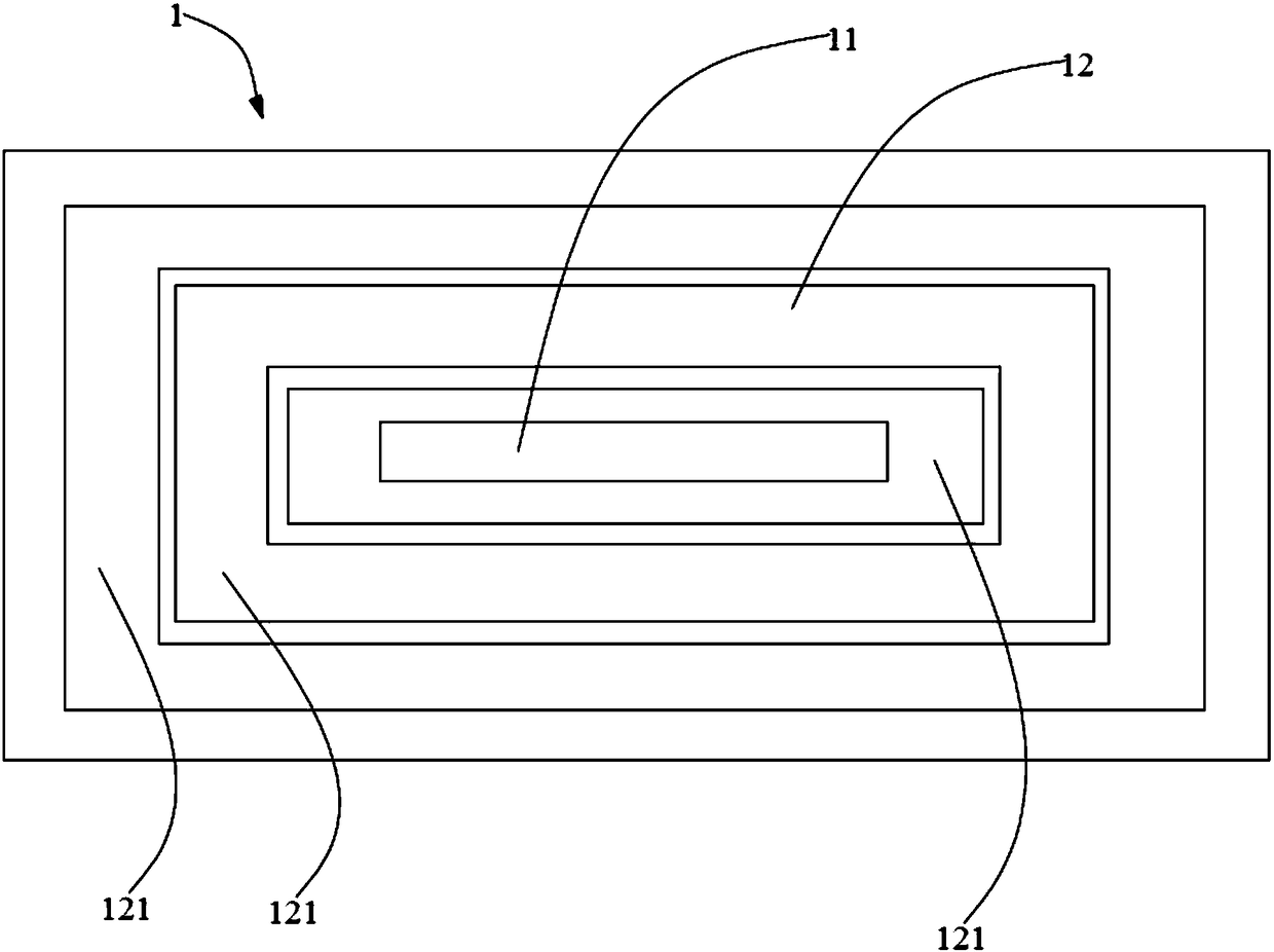
The invention provides a miniature OLED display device. The device comprises a silicon substrate, an OLED device arranged on the silicon substrate and a film packaging layer used for packaging the OLED device. The silicon substrate comprises a display area corresponding to the orthographic projection of the OLED device and a packaging area located at the periphery of the display area. The packaging area has several grooves. The film packaging layer covers the several grooves. Through using the several grooves, the permeation paths of side surface water vapor and oxygen are prolonged, the waterprevention oxygen performance of the miniature OLED display device is increased, and the service life of the miniature OLED display device is prolonged. The invention also provides a method for manufacturing the miniature OLED display device, and a technology process is simple.

Description

technical field [0001] The invention relates to the technical field of organic photoelectric devices, in particular to a micro OLED display device and a manufacturing method thereof. Background technique [0002] OLED (Organic Light-Emitting Diode, Organic Light-Emitting Diode) device has excellent performance such as fast response speed, wide viewing angle, high brightness, low power consumption, etc., and is a self-luminous device. It is considered to be a next-generation display technology with great development prospects. . [0003] Silicon-based microdisplay is a high PPI (Pixels Per Inch) display device, and its packaging methods still use three methods: cover plate type, Frit and thin film encapsulation (Thin Film Encapsulation). Effective packaging can prevent the intrusion of water vapor and oxygen, prevent the aging of organic materials, and prolong the life of OLED devices. However, no matter what the packaging method is, it is necessary to block water on the sur...

Claims


Application Information

Patent Timeline
Patent Type & Authority Applications(China)
IPC IPC(8): H01L27/32H01L51/52
CPCH10K59/12H10K50/841
Inventor 吴疆
Owner KUNSHAN FANTAVIEW ELECTRONICS TECH CO LTD
Learn More