OLED display panel and manufacturing method thereof

A technology for display panels and manufacturing methods, applied in semiconductor/solid-state device manufacturing, electrical components, electric solid-state devices, etc., can solve the problems of weak water and oxygen resistance, water and oxygen intrusion and corrosion of OLED layers, etc., and achieve improved water and oxygen resistance Effect

Active Publication Date: 2019-01-04
WUHAN CHINA STAR OPTOELECTRONICS SEMICON DISPLAY TECH CO LTD
View PDF12 Cites 4 Cited by
  • Summary
  • Abstract
  • Description
  • Claims
  • Application Information

AI Technical Summary

Problems solved by technology

[0005] The invention provides an OLED display panel and a manufacturing method thereof, which solves the problem that the water and oxygen intrusion and corrosion of the OLED layer are caused by the weak water and oxygen resistance in the side area of ​​the existing OLED display panel

Method used


Image

  • OLED display panel and manufacturing method thereof
  • OLED display panel and manufacturing method thereof
  • OLED display panel and manufacturing method thereof

Examples


Embodiment Construction

[0043] The following descriptions of the various embodiments refer to the accompanying drawings to illustrate specific embodiments in which the invention may be practiced. The directional terms mentioned in the present invention, such as [top], [bottom], [front], [back], [left], [right], [inside], [outside], [side], etc., are only for reference The orientation of the attached schema. Therefore, the directional terms used are used to illustrate and understand the present invention, but not to limit the present invention. In the figures, structurally similar elements are denoted by the same reference numerals.

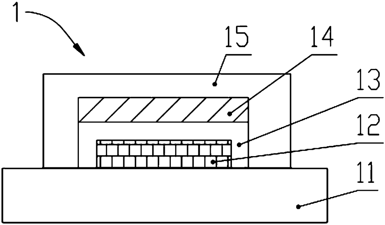
[0044] The present invention aims at the problem that the side area of ​​the existing OLED display panel has weak resistance to water and oxygen, which causes water and oxygen to intrude and corrode the OLED layer, and this embodiment can solve this defect.

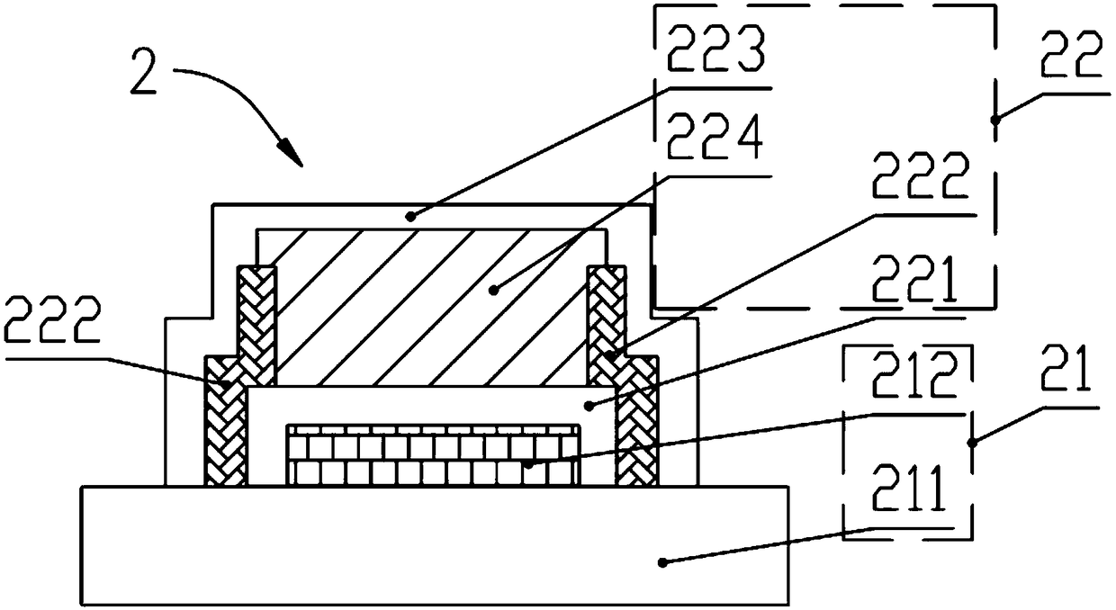
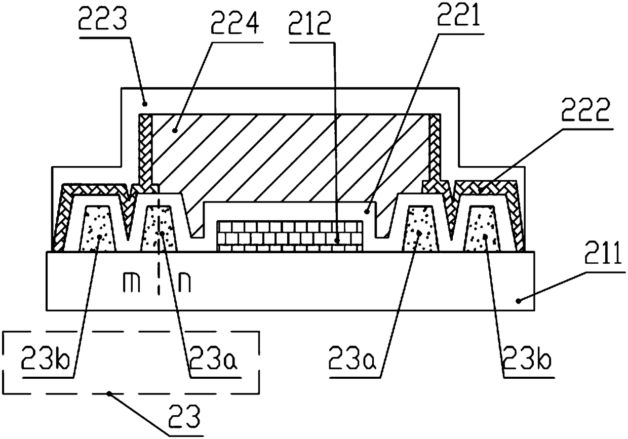
[0045] Such as figure 2 As shown, the present invention provides an OLED display panel 2 comprising: an OLED ...


PUM


Abstract

The invention provides an OLED display panel and a manufacturing method thereof, comprising an OLED substrate and a packaging part arranged on the OLED substrate. The OLED substrate comprises an arraysubstrate and an OLED layer arranged on the array substrate. The packaging part comprises: a first inorganic layer arranged on the OLED substrate and covering the OLED layer; an organic layer disposed on the first inorganic layer; A second inorganic layer disposed on a side of the first inorganic layer; and a third inorganic layer disposed on the organic layer and covering the organic layer and the second inorganic layer. The invention has the beneficial effect that an inorganic layer with high water-oxygen resistance is added to the side part of the organic layer in the packaging part, so asto improve the water-oxygen resistance of the side area of the OLED display panel.

Description

technical field [0001] The invention relates to the field of display technology, in particular to an OLED display panel and a manufacturing method thereof. Background technique [0002] An organic light emitting diode (OLED for short) has excellent characteristics such as self-illumination, low energy consumption, wide viewing angle, rich colors, and fast response, and flexible display devices can be prepared by using OLEDs. OLED has therefore aroused great interest in the scientific research community and the industry, and is considered to be a very promising next-generation technology. [0003] Such as figure 1 As shown, the OLED screen widely used in the display field currently generally adopts a top-emitting device structure, and the organic light-emitting device 12 is composed of an anode, an organic layer and a cathode. Wherein, the organic layer includes a hole injection layer, a hole transport layer, a light emitting layer, an electron transport layer, a light emit...

Claims


Application Information

Patent Timeline
Patent Type & Authority Applications(China)
IPC IPC(8): H01L51/52H01L51/56
CPCH10K50/8445H10K71/00H10K50/844H10K50/8426H10K59/87
Inventor 徐彬许红玉
Owner WUHAN CHINA STAR OPTOELECTRONICS SEMICON DISPLAY TECH CO LTD
Why Eureka
Try Eureka