Degradable substrate for flexible photoelectric device and production method of substrate

A technology for optoelectronic devices and substrates, applied in the fields of electro-solid devices, semiconductor/solid-state device manufacturing, photovoltaic power generation, etc., can solve the problems of electronic waste pollution, reduce water and oxygen penetration, etc., to improve performance, increase binding force, and reduce crystallinity. Effect

Inactive Publication Date: 2015-06-24
UNIV OF ELECTRONICS SCI & TECH OF CHINA
View PDF4 Cites 4 Cited by
  • Summary
  • Abstract
  • Description
  • Claims
  • Application Information

AI Technical Summary

Problems solved by technology

[0004] In order to solve the above technical problems, the present invention provides a degradable substrate for flexible optoelectronic devices and a preparation method thereof, which improves the flexibility of the flexible substrate, reduces the water-oxygen permeability, improves the flatness of the substrate surface, and enables The combin

Method used


Image

  • Degradable substrate for flexible photoelectric device and production method of substrate
  • Degradable substrate for flexible photoelectric device and production method of substrate

Examples


preparation example Construction

[0094] The preparation method of the degradable flexible optoelectronic device substrate is characterized in that it comprises the following steps:

[0095] ① Clean the rigid substrate with surface roughness less than 1nm, and dry it with dry nitrogen after cleaning;

[0096] ② Prepare flexible substrates on rigid substrates by roller coating, LB film method, scraping coating, spin coating, drop coating, spray coating, pulling method, casting method, dip coating, inkjet printing, self-assembly or screen printing, The flexible substrate is shellac, and the shellac is mixed with ultraviolet sensitive glue, and the composition and mass ratio of the ultraviolet sensitive glue are:

[0097] Photosensitive polysiloxane 90-98%

[0098] Photoinitiator 1-6.5%

[0099] Diluents and additives 1-4.5%;

[0100] The diluent includes toluene, xylene, active epoxy resin diluent, cyclic ether and vinyl ether monomer, and the auxiliary agent includes filler, stabilizer and crosslinking agent...

Embodiment 1

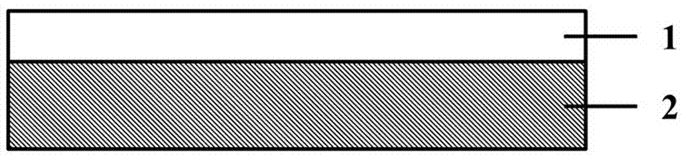
[0106] Such as figure 1 The substrate structure shown includes a flexible substrate 2 and a conductive layer 1, the flexible substrate 2 is shellac doped with UV-sensitive glue, and the conductive layer 1 is graphene.

[0107] The preparation method is as follows:

[0108] ① Clean the rigid substrate with surface roughness less than 1nm, and dry it with dry nitrogen after cleaning;

[0109] 2. on the rigid substrate, adopt spin coating to prepare shellac and UV-sensitive glue mixed film (the mass ratio of UV-sensitive glue is 0.5%), and film thickness is 50 μ m, and the raw material of described UV-sensitive glue comprises following composition:

[0110] Photosensitive polysiloxane 90%

[0111] Photoinitiator 6.5%

[0112] Diluents and additives 3.5%;

[0113] ③ Prepare a conductive layer from the graphene aqueous dispersion in ② surface spraying method, with a height of 20cm, a spraying pressure of 0.3MPa, a spraying rate of 0.3mL / min, and a thickness of the conductive la...

Embodiment 2

[0119] Such as figure 1 The substrate structure shown includes a flexible substrate 2 and a conductive layer 1, the flexible substrate 2 is shellac doped with ultraviolet sensitive glue, and the conductive layer 1 is carbon nanotubes.

[0120] The preparation method is as follows:

[0121] ① Clean the rigid substrate with surface roughness less than 1nm, and dry it with dry nitrogen after cleaning;

[0122] 2. on the rigid substrate, adopt spin coating to prepare shellac and UV-sensitive glue mixed film (the mass ratio of UV-sensitive glue is 1%), and film thickness is 100 μ m, and the raw material of described UV-sensitive glue comprises following composition:

[0123] Photosensitive polysiloxane 92%

[0124] Photoinitiator 3.5%

[0125] Diluents and auxiliaries 4.5%;

[0126] ③ Prepare a conductive layer with carbon nanotube aqueous dispersion in ② surface spraying method, with a height of 20cm, a spraying pressure of 0.3MPa, a spraying rate of 0.3mL / min, and a thickness...


PUM

PropertyMeasurementUnit
Surface roughnessaaaaaaaaaa
Thicknessaaaaaaaaaa
Resistanceaaaaaaaaaa

Abstract

The invention discloses a degradable substrate for a flexible photoelectric device and a production method of the substrate. The substrate comprises a flexible substrate and a conductive layer, wherein the conductive layer is located on the flexible substrate, and the flexible substrate is shellac doped with ultraviolet-sensitive adhesive; the ultraviolet-sensitive adhesive comprises photosensitive polysiloxane, photoinitiator, thinner and promoter; the thinner comprises methylbenzene, xylene, active epoxy resin thinner, cyclic ether and vinyl ether monomer; the promoter comprises filler, stabilizer and cross-linking agent. The degradable substrate has the advantages that the light transmittance of the flexible substrate is increased by the cross-linking effect of the ultraviolet-sensitive adhesive, the toughness of the flexible substrate is increased, and the combining force of the conductive layer and the flexible substrate is strong at the same time; in addition, the substrate is biodegradable and is widely applicable to the field of flexible photoelectric devices.

Description

technical field [0001] The invention belongs to the technical field of organic optoelectronics, and in particular relates to a degradable substrate for flexible optoelectronic devices and a preparation method thereof. Background technique [0002] In recent years, flexible optoelectronic devices have been greatly developed, including flexible organic electroluminescent devices and flexible organic solar cells. With the gradual breakthrough of relevant bottleneck technologies and the gradual improvement of the industrial chain, many domestic and foreign companies are preparing to mass-produce flexible optoelectronic devices. However, with the increasing development of technology, many problems have also been brought. First of all, the conventional rigid substrates used in optoelectronic devices cannot meet people's requirements for portability and lightness; secondly, an increasing number of optoelectronic products have caused a large amount of solid pollution due to their n...

Claims


Application Information

Patent Timeline
IPC IPC(8): H01L51/44H01L51/48H01L51/46H01L51/52H01L51/56H01L51/54
CPCY02E10/549
Inventor 于军胜王煦周殿力韩世蛟
Owner UNIV OF ELECTRONICS SCI & TECH OF CHINA
Why Eureka
Try Eureka