Nitride semiconductor substrate and method for manufacturing the same, and nitride semiconductor device using nitride semiconductor substrate

a technology of nitride semiconductor and substrate, which is applied in the direction of crystal growth process, semiconductor laser, polycrystalline material growth, etc., can solve the problems of difficult to secure a region large enough for forming the device, abnormal growth, and inability to handle the same way as an ordinary single crystal substrate, so as to achieve easy control of the protective film depth and mitigate the degradation of the crystallinity of the nitride semiconductor

Inactive Publication Date: 2005-03-01
NICHIA CORP
View PDF22 Cites 61 Cited by
  • Summary
  • Abstract
  • Description
  • Claims
  • Application Information

AI Technical Summary

Benefits of technology

[0023]The protective film may be removed by dry etching or wet etching, in either way the protective film can be removed without degrading the crystallinity of the nitride semiconductor. Dry etching is capable of easily controlling the depth of the protective film to be removed.
[0024]When the protective film is removed so as to expose the surface of the supporting substrate, the problems caused by the decomposition of the protective film while growing the nitride semiconductor on the protective film, namely abnormal growth and degradation of crystallinity of the nitride semiconductor can be mitigated.

Problems solved by technology

However, in case the protective film of SiO2 or the like has wide stripe width, lateral growth of the nitride semiconductor on the protective film does not fully proceed eventually resulting in abnormal growth.
As a result, even when a single continuous nitride semiconductor substrate is formed by growing nitride semiconductor layer laterally on a protective film by the vapor phase deposition process, it cannot be handled in the same way as an ordinary single crystal substrate.
Since the active layer of a semiconductor laser should keep clear of the vicinity of the joint, it is difficult to secure a region large enough for forming the device.
Moreover, since surface of the single nitride semiconductor substrate appears to be uniform, it has been difficult to recognize the joint by viewing the top surface of the substrate and to carry out the formation of device pattern accurately.
Furthermore, in case a single continuous nitride semiconductor substrate is formed by growing nitride semiconductor laterally by using a protective film on sapphire or the like, such a structure is likely to warp.
However, it has not been easy to remove a different-material substrate such as sapphire as it takes a long time to remove by polishing or by means of excimer laser.

Method used


Image

  • Nitride semiconductor substrate and method for manufacturing the same, and nitride semiconductor device using nitride semiconductor substrate
  • Nitride semiconductor substrate and method for manufacturing the same, and nitride semiconductor device using nitride semiconductor substrate
  • Nitride semiconductor substrate and method for manufacturing the same, and nitride semiconductor device using nitride semiconductor substrate

Examples


embodiment 2

iew showing a process for manufacturing a nitride semiconductor substrate of

[0039]FIGS. 9A and 9B are sectional views schematically showing a manufacturing process to form a device on the nitride semiconductor substrate shown in FIG. 8.

[0040]FIG. 10 is a sectional view schematically showing a nitride semiconductor device using a nitride semiconductor substrate of another example of Embodiment 2.

[0041]FIG. 11 is a sectional view schematically showing a nitride semiconductor device using a nitride semiconductor substrate of still another example of Embodiment 2.

[0042]FIGS. 12A and 12B are sectional views schematically showing a nitride semiconductor substrate of Embodiment 3.

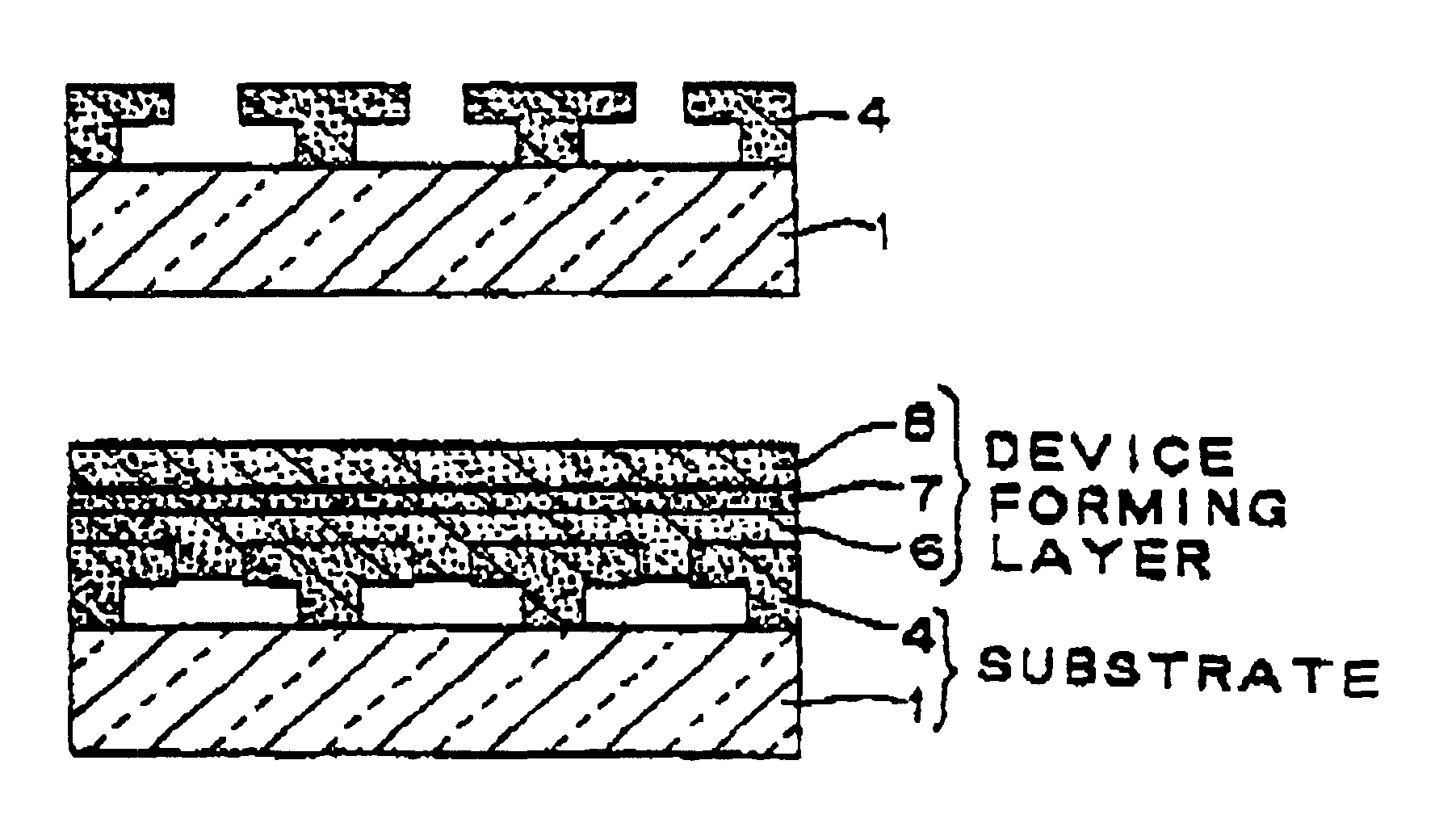
[0043]FIG. 13 is a schematic sectional view of the nitride semiconductor substrate in FIG. 6 showing more detail of the joint portion.

[0044]FIG. 14A and FIG. 14B are CL images of the nitride semiconductor substrate in Example 6 (FIG. 14A) and Comparable example 1 (FIG. 14B).

BEST MODE FOR CARRYING OUT THE INVENTION...

example 1

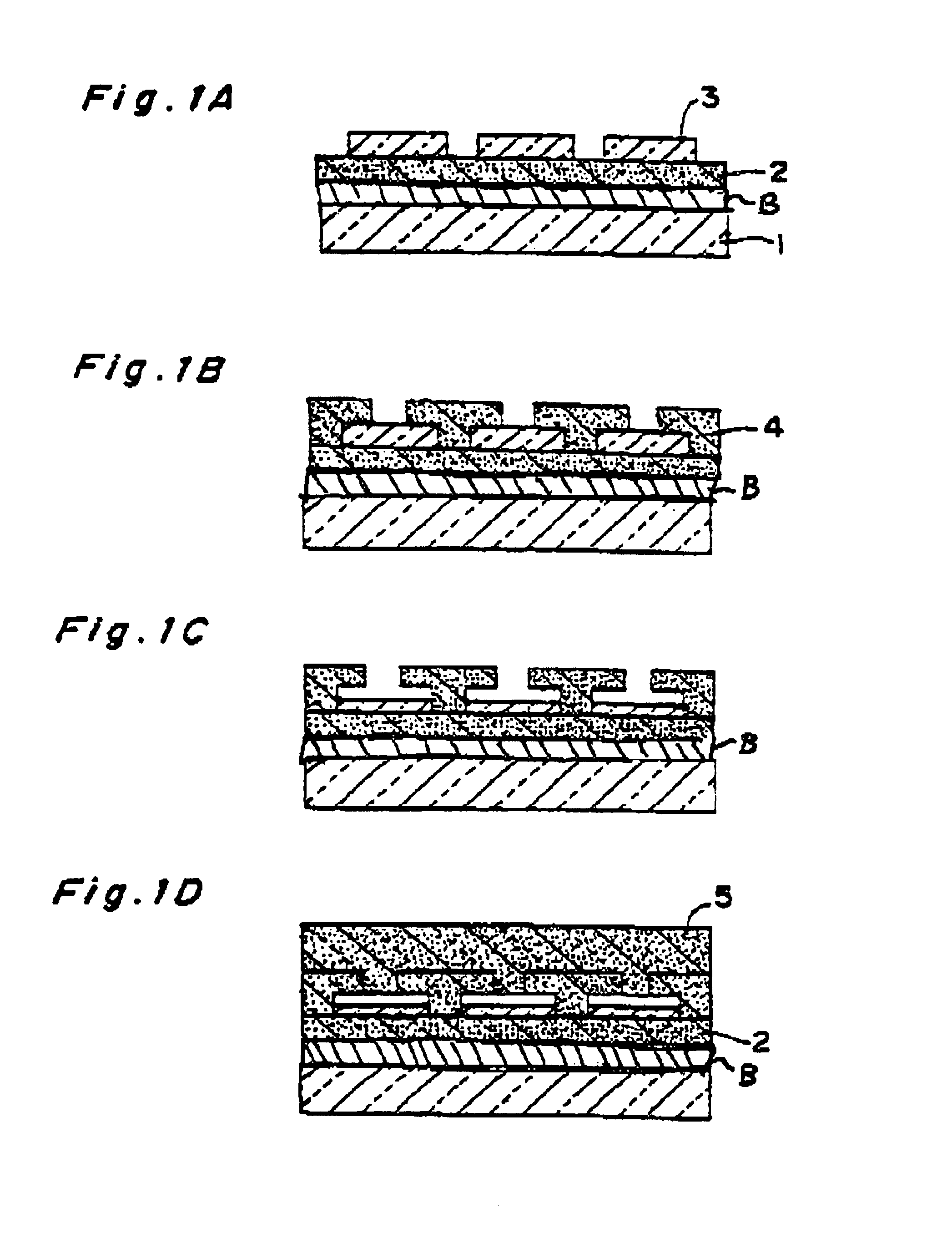
[0097]A sapphire substrate 1 having principal plane in C plane and orientation flat surface in A plane is used. A buffer layer of GaN is formed to a thickness of 200 Å on the sapphire substrate 1 at a temperature of 510° C. by MOCVD process using hydrogen as the carrier gas and ammonia and TMG (trimethyl-gallium) as the stock material gas.

[0098]After growing the buffer layer, supply of only the TMG is stopped and the temperature is raised to 1050° C. When the temperature has reached 1050° C., nitride semiconductor 2 made of undoped GaN is grown to a thickness of 2.5 μm by using TMG, ammonia and silane gas as the stock material gas.

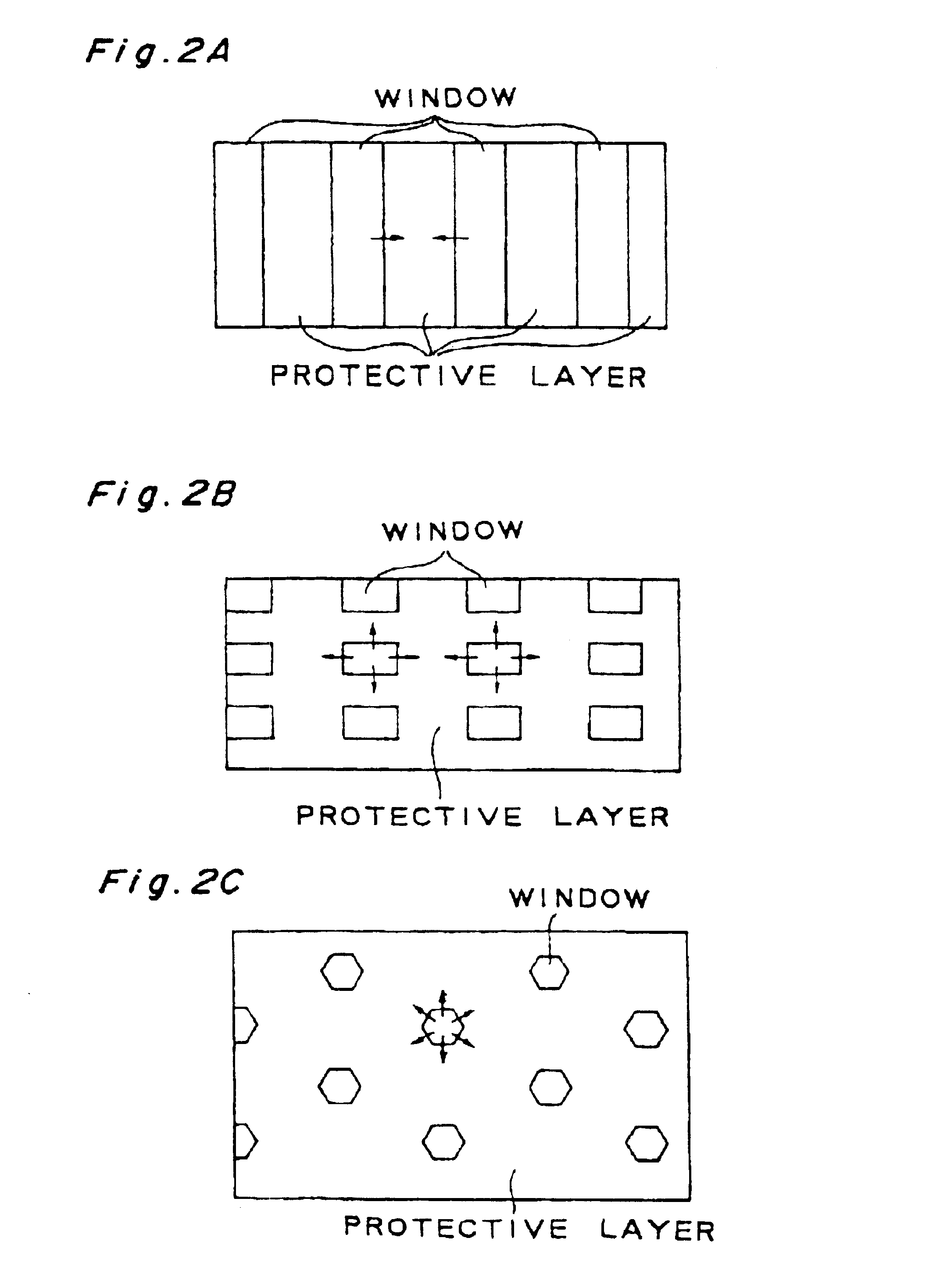
[0099]A protective film 3 made of SiO2 is formed to a thickness of 0.5 μm by the CVD process on the nitride semiconductor 2 and, after forming a photo-mask of stripe configuration, the protective film 3 made of SiO2 having stripe width of 14 μm and window size of 6 μm is formed by etching. Direction of the stripes of the protective film 3 is set perpendicu...

example 2

[0104]A sapphire substrate 1 having principal plane in C plane and orientation flat surface in A plane is used. A buffer layer of GaN is formed to a thickness of 200 Å on the sapphire substrate 1 at a temperature of 510° C. by the MOCVD process using hydrogen as the carrier gas and ammonia and TMG (trimethyl-gallium) as the stock material gas.

[0105]After growing the buffer layer, a protective film 3 made of SiO2 is formed on the buffer layer to a thickness of 0.5 μm by the CVD process and, after forming a photo-mask of stripe configuration, the protective film made of SiO2 having stripe width of 14 μm and window size of 6 μm is formed by etching. Direction of the stripes of the protective film 3 is set perpendicular to the sapphire A plane.

[0106]Then the first nitride semiconductor 4 made of GaN is grown to a thickness of 15 μm at a temperature of 1050° C. under a reduced pressure by the MOCVD process using TMG, ammonia, silane gas and Cp2Mg (cyclopentadienyl magnesium) as the stock...


PUM

PropertyMeasurementUnit
melting pointaaaaaaaaaa
thicknessaaaaaaaaaa
thicknessaaaaaaaaaa

Abstract

A nitride semiconductor substrate including (a) a supporting substrate, (b) a first nitride semiconductor layer having a periodical T-shaped cross-section, having grown from periodically arranged stripe-like, grid-like or island-like portions on the supporting substrate, and (c) a second nitride semiconductor substrate covering said supporting substrate, having grown from the top and side surfaces of said first nitride semiconductor layer, wherein a cavity is formed under the second nitride semiconductor layer.
A protective layer having a periodically arranged stripe-like, grid-like or island-like apertures is formed on the supporting substrate. The first nitride semiconductor layer is laterally grown from the exposed portion of the substrate. The growth is stopped before the first nitride semiconductor layer covers the supporting substrate. Thus, the first nitride semiconductor layer has a periodical T-shaped cross-section. Then, the protective layer is removed and the second nitride semiconductor layer is grown from the top and side surface of the first nitride semiconductor layer to cover the substrate.

Description

[0003]This application is a Division of Ser. No 09 / 880,843 filed Jun. 15, 2001, now U.S. Pat. No. 6,627,974.TECHNICAL FIELD[0004]The present invention relates to a method for growing a nitride semiconductor (InxAlyGa1−x−yN, 0≦X, 0≦Y, X+Y≦1), and particularly to a method for growing a nitride semiconductor which can be used to make a nitride semiconductor substrate.BACKGROUND ART[0005]Recently various researches have been conducted on the growth of nitride semiconductor on a substrate made of a different material such as sapphire, spinel or silicon carbide which has a lattice constant different from that of the nitride semiconductor.[0006]For example, a method of growing epitaxial lateral overgrowth GaN (ELOG) is described in JPN. J. Appl. Phys., vol.37 (1998), pp. L309-L312, wherein nitride semiconductor having lower density of dislocations is obtained by forming a protective film of SiO2 or other material partially on a nitride semiconductor which has been grown on the C plane of s...

Claims


Application Information

Patent Timeline
Patent Type & Authority Patents(United States)
IPC IPC(8): C30B25/18C30B25/02H01L21/20H01L21/02H01S5/323H01S5/00H01S5/02
CPCC30B25/02C30B29/403C30B29/406H01L21/0237H01L21/0242H01L21/02433H01L21/02458H01L21/0254H01L21/02579H01L21/02639H01L21/02642H01L21/02647H01S5/32341C30B25/18H01S2304/12H01S5/0217H01S5/3063H01L21/205
Inventor KOZAKI, TOKUYAKIYOKU, HIROYUKICHOCHO, KAZUYUKIMAEGAWA, HITOSHI
Owner NICHIA CORP
Why Eureka
Try Eureka