Schottky barrier diode and integrated circuit using the same

a barrier diode and integrated circuit technology, applied in the direction of basic electric elements, electrical apparatus, semiconductor devices, etc., can solve the problems of high breakdown voltage, low resistance of sbd, low etc., to prevent the breakdown voltage of sbd

Active Publication Date: 2006-05-25
PANASONIC CORP
View PDF11 Cites 61 Cited by
  • Summary
  • Abstract
  • Description
  • Claims
  • Application Information

AI Technical Summary

Benefits of technology

[0024] In this manner, in the Schottky barrier diode and the integrated circuit of this invention, it is possible to prevent lowering of the breakdown voltage of the SBD and different voltages can b...

Problems solved by technology

On the contrary, when a nitride material such as GaN with a high breakdown voltage is used, an SBD can attain a high breakdown voltage even when the thickness of a drift layer is decreased, and therefore, such an SBD attains a low on resistance and a high breakdown voltage.
The conventional SBDs have, however, the following problems: The first problems is caused because the depletion layer extends, in applying a backward bias voltage, to the peripheral portion of the SBD where a large number of crystal defects are caused by mechanical damage occurring in dici...

Method used


Image

  • Schottky barrier diode and integrated circuit using the same
  • Schottky barrier diode and integrated circuit using the same
  • Schottky barrier diode and integrated circuit using the same

Examples


modification 1 if embodiment 1

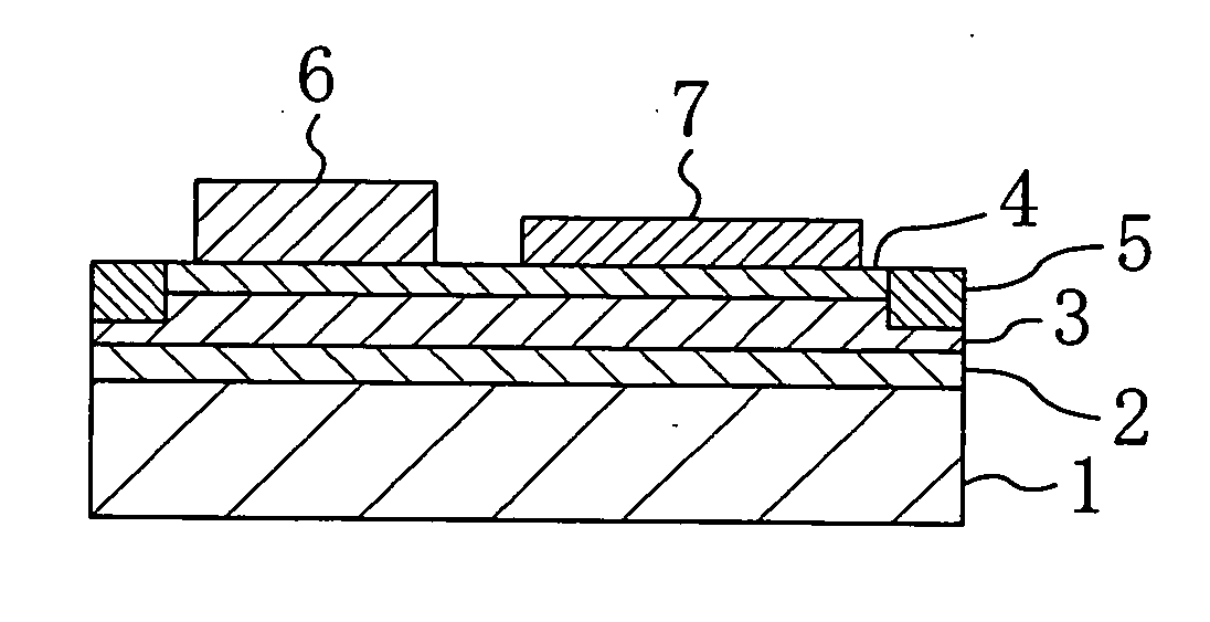
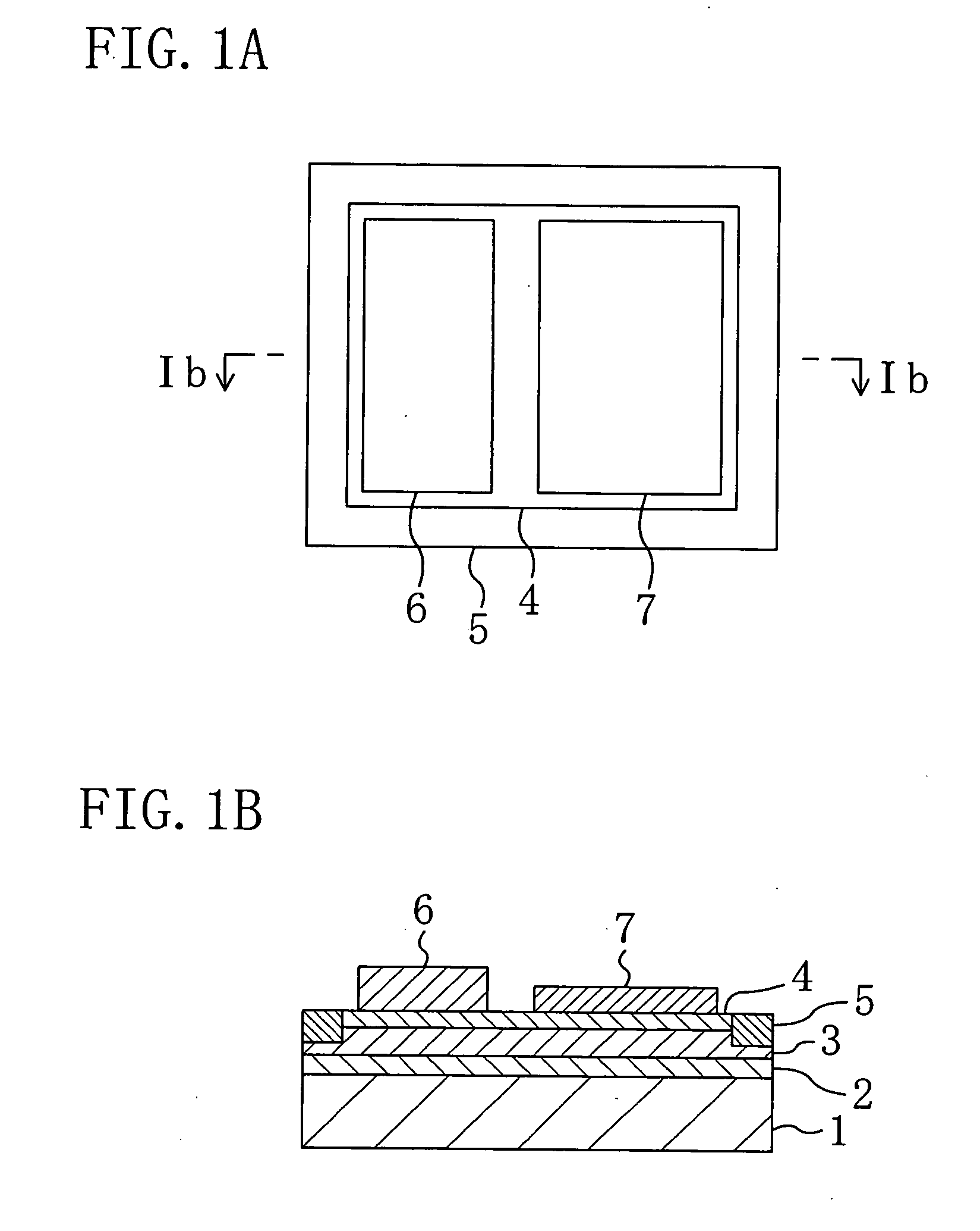
[0048] An SBD according to Modification 1 of Embodiment 1 will now be described with reference to the accompanying drawings. FIGS. 4A and 4B show the structure of the SBD of this modification, and specifically, FIG. 4A is a plan view thereof and FIG. 4B is a cross-sectional view-thereof taken on line IVb-IVb of FIG. 4A. In FIGS. 4A and 4B, like reference numerals are used to refer to like elements shown in FIGS. 1A and 1B so as to omit the description.

[0049] As shown in FIG. 4A, the SBD of this modification includes a Schottky electrode 6 having an outline in a square shape in the plan view, and the Schottky electrode 6 is formed to surround an ohmic electrode 7 formed in a square shape in the plan view at the center. In an SBD utilizing a two-dimensional electron gas, a forward current flows in parallel to a substrate between a Schottky electrode and an ohmic electrode. Accordingly, in order to allow a large current to flow in the SBD, it is necessary to make as long as possible a...

modification 2

of Embodiment 1

[0052]FIGS. 5A and 5B show the structure of an SBD according to Modification 2 of Embodiment 1, and specifically, FIG. 5A is a plan view thereof and FIG. 5B is a cross-sectional view thereof taken on line Vb-Vb of FIG. 5A. In FIGS. 5A and 5B, like reference numerals are used to refer to like elements shown in FIGS. 1A and 1B so as to omit the description. As shown in FIGS. 5A and 5B, in the SBD of this modification, a Schottky electrode 6 does not completely surround an ohmic electrode 7 but has a cut portion.

[0053] In the case where the Schottky electrode 6 has the cut portion in this manner, although the length of an opposing portion between the ohmic electrode 7 and the Schottky electrode 6 is shorter, the lift-off can be more easily performed in forming the Schottky electrode 6 than in Modification 1 of Embodiment 1. Therefore, this SBD can be more easily fabricated.

embodiment 2

[0054] An integrated circuit according to Embodiment 2 of the invention will now be described with reference to the accompanying drawings. FIG. 6 shows an equivalent circuit of the integrated circuit of this embodiment. FIGS. 7A and 7B show the structure of the integrated circuit of this embodiment, and specifically, FIG. 7A is a plan view thereof and FIG. 7B is a cross-sectional view thereof taken on line VIIb-VIIb of FIG. 7A.

[0055] As shown in FIG. 6, the integrated circuit of this embodiment is a voltage limiter circuit in which a first SBD 21A and a second SBD 21B are connected to each other in reverse directions. When a voltage applied between an input terminal 41 and an input terminal 42 exceeds the on voltage in the forward direction of the SBDs, a current flows through the SBDs, and hence, a voltage between an output terminal 43 and an output terminal 44 never exceeds the on voltage of the SBDs.

[0056] As shown in FIGS. 7A and 7B, a buffer layer 12 of aluminum nitride (AlN)...


PUM


Abstract

A Schottky barrier diode includes a first semiconductor layer and a second semiconductor layer successively formed above a substrate; and a high-resistance region formed in the first semiconductor layer and the second semiconductor layer and having higher resistance than the first semiconductor layer and the second semiconductor layer. A Schottky electrode and an ohmic electrode spaced from each other are formed on the second semiconductor layer in a portion surrounded with the high-resistance region.

Description

CROSS-REFERENCE TO RELATED APPLICATIONS [0001] This application claims priority under 35 U.S.C. § 119 on patent application No. 2004-338015 filed in Japan on Nov. 22, 2004, the entire contents of which are hereby incorporated by reference.BACKGROUND OF THE INVENTION [0002] The present invention relates to a Schottky barrier diode using a nitride semiconductor material and an integrated circuit using the same. [0003] Nitride semiconductors typified by GaN are being earnestly developed for application to electronic devices such as a field effect transistor (FET) and a Schottky barrier diode (SBD) by taking advantage of their merits such as a high breakdown voltage and a high saturated electronic velocity. An SBD is required to have a high breakdown voltage and a low on resistance, and in order to realize a high breakdown voltage in a conventional SBD using a silicon (Si) material, it is necessary to lower a carrier concentration and increase the thickness of a drift layer where a depl...

Claims


Application Information

Patent Timeline
IPC IPC(8): H01L29/739
CPCH01L29/66143H01L29/872
Inventor YANAGIHARA, MANABUUEMOTO, YASUHIROTANAKA, TSUYOSHIUEDA, DAISUKE
Owner PANASONIC CORP
Why Eureka
Try Eureka