Circuit board with symmetrical bonding pads

A symmetrical soldering and circuit board technology, applied to printed circuits, printed circuits, printed circuit components, etc., can solve problems such as virtual soldering, uneven lighting, and uneven distances

Pending Publication Date: 2018-07-24
江门黑氪光电科技有限公司
View PDF0 Cites 4 Cited by
  • Summary
  • Abstract
  • Description
  • Claims
  • Application Information

AI Technical Summary

Problems solved by technology

[0003] Since the positive and negative poles of the LED lamp have a large and small structure, the traditional positive and negative pads are also set to a large and small structure. The outer contour is larger than the outer contour of the LED lamp, so that during the process of heating the solder paste and flux to melt, the LED lamp will float on the solder paste, causing the LED lamp to shift. The size of the paste is different, and the shrinkage stress of the positive lamp pin and the negative lamp pin of the LED lamp is different, which will cause the LED lamp to be pulled and then shifted, which may cause the distance between the LED lamps on the LED lamp strip to be unequal, resulting in uneven light emission , in severe cases, it will cause the lamp pin to separate from the pad, resulting in false welding and dead light

Method used


Image

  • Circuit board with symmetrical bonding pads
  • Circuit board with symmetrical bonding pads
  • Circuit board with symmetrical bonding pads

Examples


Embodiment Construction

[0017] The technical solutions of the present invention will be described below with reference to the accompanying drawings and embodiments.

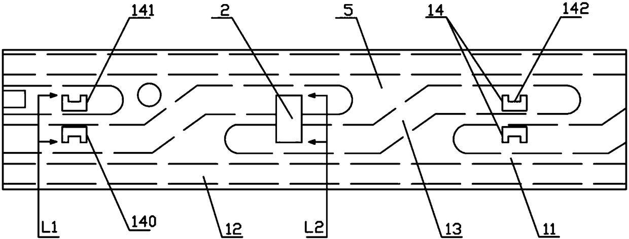
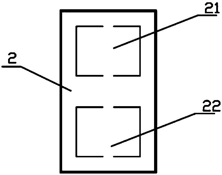
[0018] like figure 1 and figure 2 As shown, a circuit board with symmetrical pads according to the present invention includes a circuit board, and the circuit board 1 includes an insulating layer, a circuit layer 5 arranged on the insulating layer, and a solder resist covering the circuit layer 5 Layer 11, the position where the LED lamp 2 needs to be welded on the solder mask layer 11 is provided with an LED lamp bead pad 14, and the LED lamp bead pad 14 includes symmetrically arranged positive electrode pad 141 and negative electrode pad 140, positive electrode pad 141 and negative electrode The shape and size of the pads 140 are the same, and the outer contour L1 of the positive electrode pad 141 and the negative electrode pad 140 is smaller than or equal to the outer contour L2 of the LED lamp to be welded. With such a structure,...


PUM


Abstract

The invention relates to the technical field of LED circuit boards, and particularly relates to a circuit board with symmetrical bonding pads. The circuit board with symmetrical bonding pads comprisesa circuit board, wherein the circuit board comprises an insulating layer, a circuit layer arranged on the insulating layer and a solder mask covering the circuit layer, the solder mask is provided with an LED lamp bead bonding pad at each part where an LED lamp is required to be welded, each LED lamp bead bonding pad comprises a positive electrode bonding pad and a negative electrode bonding padwhich are symmetrically arranged, the positive electrode bonding pad and the negative electrode bonding pad are the same in shape and size, and the outer contour of the positive electrode bonding padand the negative electrode bonding pad is less than or equal to the outer contour of an LED lamp required to be welded. The outer contour of the positive electrode bonding pad and the negative electrode bonding pad is less than or equal to the outer contour of the LED lamp required to be welded, and positive electrode bonding pad and the negative electrode bonding pad are the same as lamp pins ofthe LED lamp required to be welded in shape and size, thereby effectively preventing the LED lamps from floating and shifting in the process of heating and melting a solder paste flux, thus enabling the LED lamps on an LED lamp strip to be equal in spacing and uniform in light emitting, and being capable of reducing the generation rate of faulty soldering.

Description

technical field [0001] The invention relates to the technical field of LED circuit boards, in particular to a circuit board with symmetrical pads. Background technique [0002] The LED light strip is composed of a circuit board and an outer skin, and the LED light is welded on the circuit board. The lower layer of the circuit board is an insulating layer, and the middle layer is a circuit layer. The circuit layer is provided with a positive and negative power supply circuit and an LED lamp bead series circuit. Positive and negative pads are opened. The process of soldering the LED lamp to the circuit board is as follows: first drop the solder paste into the pad, and then align the positive and negative poles of the LED lamp with the positive and negative pads to fix it. After heating, the flux in the solder paste melts. Volatile, the solder paste precipitation fixes the positive and negative lamp pins of the LED lamp and makes the lamp pins electrically connect with the ci...

Claims


Application Information

Patent Timeline
Patent Type & Authority Applications(China)
IPC IPC(8): H05K1/11
CPCH05K1/111H05K2201/10106
Inventor 赖思强
Owner 江门黑氪光电科技有限公司
Why Eureka
Try Eureka