Inductor stacking structure

A stacking structure and inductance technology, applied in the direction of inductors, transformer/inductor components, circuits, etc., can solve problems affecting circuit integration, size and manufacturing costs, low quality factor of inductance, affecting circuit performance, etc., to reduce parasitic Capacitance, high inductance and quality factor, effect of reduced area

Pending Publication Date: 2018-07-31
ANHUI YUNTA ELECTRONICS TECH CO LTD
View PDF0 Cites 9 Cited by
  • Summary
  • Abstract
  • Description
  • Claims
  • Application Information

AI Technical Summary

Problems solved by technology

At this stage, there are often two problems with inductors in integrated circuits. One is that the quality factor (Q value) of the inductor is low, which will affect the circuit performance; the other is that the inductor has a large area, which will affect the circuit integration, size and production. cost

Method used


Image

  • Inductor stacking structure
  • Inductor stacking structure
  • Inductor stacking structure

Examples


Embodiment Construction

[0023] The present invention will be further described in detail below in conjunction with the accompanying drawings and embodiments. It should be understood that the specific embodiments described here are only used to explain the present invention, but not to limit the present invention. In addition, it should be noted that, for the convenience of description, only some structures related to the present invention are shown in the drawings but not all structures.

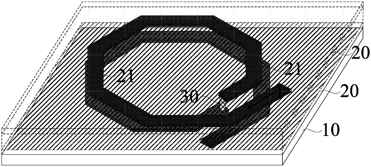
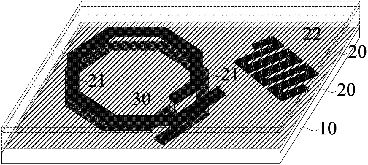
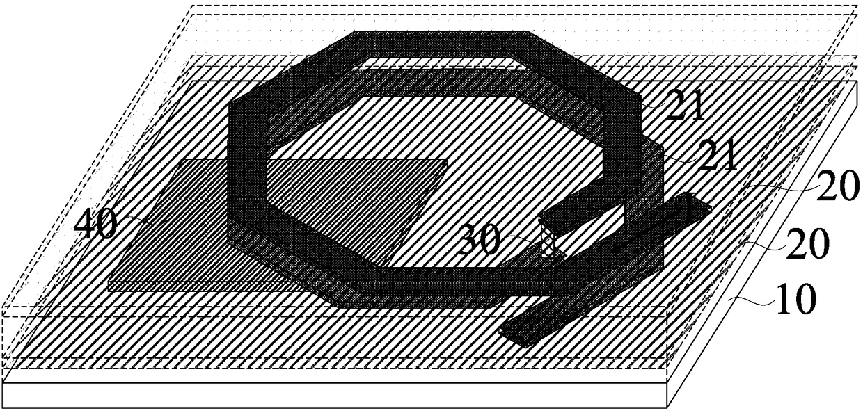
[0024] figure 1 It is a structural schematic diagram of an inductor stack structure provided by an embodiment of the present invention. see figure 1 , the inductor stack structure provided by the embodiment of the present invention includes: a substrate 10; at least two metal layers 20 stacked on one side of the substrate 10 in sequence, and each layer of metal layer 20 includes at least a first planar inductor 21; through holes 30 located at any Between two adjacent metal layers 20 , the first planar inductors ...


PUM


Abstract

The present invention discloses an inductor stacking structure. The inductor stacking structure comprises: a substrate; at least two metal layers stacked at one side of the substrate in order, each metal layer at least comprising one first planar inductor; through holes located between any two adjacent metal layers, wherein the first planar inductors in different metal layers are electrically connected through the through holes, and the thickness of the through holes is larger than the thickness of the metal layers. The multiple metal layers with the first planar inductors are arranged to increase the inductance values of the inductors in the inductor stacking structure, the through holes with the thickness larger than the thickness of the metal layers are employed to connect the first planar inductors in the metal layers to reduce the interference among the first planar inductors. Compared to the prior art, in a condition that the mutual inductance among the fist planar inductors in the different metal layers is not greatly reduced, stray capacitance between the different metal layers can be greatly reduced to allow the inductor to keep a high inductance value and a quality factorwhen the inductor has a small area and reduce the area of an integration circuit.

Description

technical field [0001] Embodiments of the present invention relate to integrated circuit technology, and in particular to an inductor stack structure. Background technique [0002] With the increasing development of electronic products, the research and development of various components are moving towards the direction of high integration and multi-function. Therefore, the requirements for the integrated circuit structure of the device are also increasing. [0003] Inductor design is often a difficult problem in integrated circuit design. At this stage, there are often two problems with inductors in integrated circuits. One is that the quality factor (Q value) of the inductor is low, which will affect the circuit performance; the other is that the inductor has a large area, which will affect the circuit integration, size and production. cost. Contents of the invention [0004] The invention provides an inductance stacking structure to achieve the purpose of reducing the ...

Claims


Application Information

Patent Timeline
Patent Type & Authority Applications(China)
IPC IPC(8): H01L23/522H01F27/28H01F27/34
CPCH01L23/5227H01F27/2871H01F27/34H01L28/10
Inventor 程伟左成杰何军
Owner ANHUI YUNTA ELECTRONICS TECH CO LTD
Why Eureka
Try Eureka