An inductance structure used in printed circuit board embedding technology and its manufacturing method

A printed circuit board and manufacturing method technology, applied in directions containing printed inductors, printed electrical components, etc., can solve problems such as instability and low inductance value, and achieve increased inductance value, reduced occupied area, and improved micro degree of effect

Active Publication Date: 2018-09-21
UNIV OF ELECTRONICS SCI & TECH OF CHINA
View PDF15 Cites 0 Cited by
  • Summary
  • Abstract
  • Description
  • Claims
  • Application Information

AI Technical Summary

Problems solved by technology

[0006] Aiming at the technical problem of low and unstable inductance value existing in the existing embedded magnetic core inductance structure, the present invention provides an inductance structure for printed circuit board PCB embedding technology and a manufacturing method thereof

Method used


Image

  • An inductance structure used in printed circuit board embedding technology and its manufacturing method
  • An inductance structure used in printed circuit board embedding technology and its manufacturing method
  • An inductance structure used in printed circuit board embedding technology and its manufacturing method

Examples


Embodiment 1

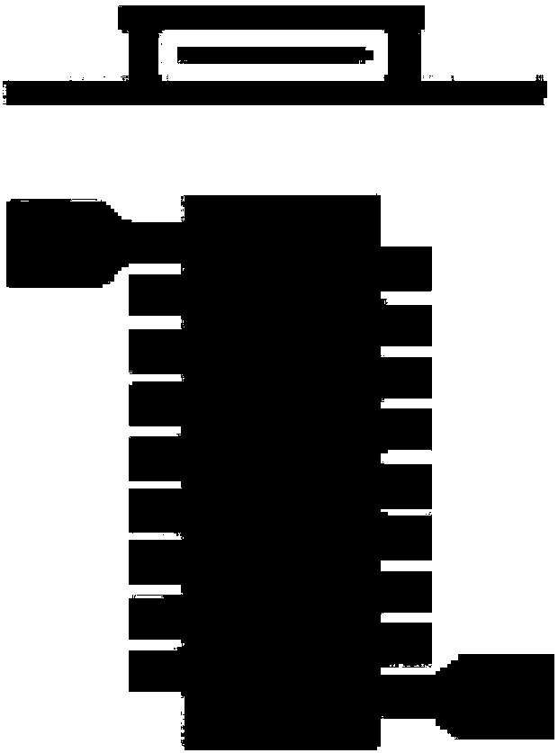
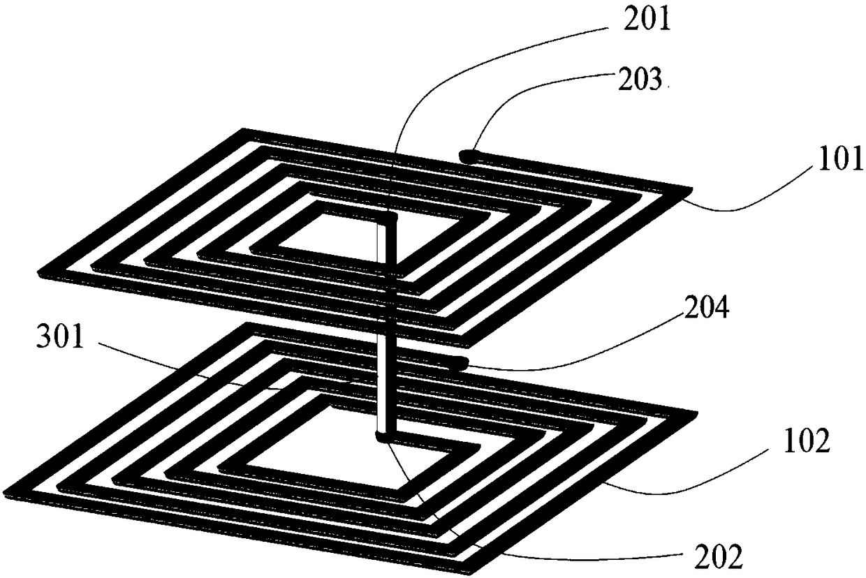
[0044] An inductance structure used in printed circuit board embedding technology, including a first conductive coil 101 and a second conductive coil 102 respectively etched on the top and bottom surfaces of a double-sided copper-clad substrate and a magnetic core located in the two wire coils 7. The inner ends of the first conductive coil 101 coincide with the inner ends of the two conductive coils in the vertical projection formed by the plane where the second conductive coil 102 is located, and the inner ends of the first conductive coil 101 and the inner ends of the second conductive coil 102 A first pad 201 and a second pad 202 are respectively provided, and the first conductive coil 101 and the second conductive coil 102 are arranged between the first pad 201 and the second pad 202 The via hole 301 is connected, and the inner wall of the via hole 301 is coated with a uniform metal layer such as ( image 3 As shown), the non-copper-clad region 1 601 and the non-copper-cla...

Embodiment 2

[0050] A method for manufacturing an inductance structure used in printed circuit board embedding technology, characterized in that it comprises the following steps:

[0051] Step A: After pattern transfer is performed on the top and bottom surfaces of the double-sided copper-clad substrate, the first conductive coil 101 and the second conductive coil 102 are obtained by etching, wherein: the first conductive coil 101 is formed on the plane where the second conductive coil 102 is located In the vertical projection of , the inner ends of the two conductive coils overlap and the single-turn coil in one conductive coil and the single-turn coil in the other conductive coil are arranged alternately from inside to outside to form a tight winding structure;

[0052] Step B: using a numerical control drilling machine to drill a via hole for communication between the first conductive coil 101 and the second conductive coil 102 prepared in step A, and then metallize the inner wall of the...


PUM


Abstract

The invention provides an inductance structure used in printed circuit board embedding technology and its manufacturing method, which belongs to the technical field of printed circuit integrated components. The invention improves the structure of the magnetic core and the winding method of the coil to improve the inductance value and the stability of the inductance during use; the inductance structure provided by the invention can reduce the occupied area of ​​the copper coil on the PCB substrate, improve the miniaturization of the size of the inductance element, and make the inductance structure small in size and high in performance; the present invention mainly The inductance structure used in the embedded inductance technology of printed circuit boards is formed by using graphic transfer technology, interlayer through holes, window opening treatment, electroplating and chemical plating, and hot-pressed layering. The manufacturing method is simple and highly controllable. Compatible with the process of the existing printed circuit board technology, it is beneficial to improve the integration degree of printed circuit components.

Description

technical field [0001] The invention belongs to the technical field of printed circuit integrated components, in particular to an inductance structure used in printed circuit board embedding technology and a manufacturing method thereof. Background technique [0002] The development trend of miniaturization and thinning of multi-functional electronic information products requires that printed circuit products equipped with components and realize electrical transmission show a higher degree of integration. internal. In addition to reducing the area occupied by the components on the board and reducing the three-dimensional size of electronic information products, the printed circuit board with integrated components can realize the minimum distance transmission of electrical signals because the components are embedded in the printed circuit board. It eliminates the attenuation problem of the printed circuit signal to the greatest extent and improves the integrity of signal tra...

Claims


Application Information

Patent Timeline
Patent Type & Authority Patents(China)
IPC IPC(8): H05K1/16
CPCH05K1/165
Inventor 何雪梅何为陈苑明王守绪周国云王翀申桃
Owner UNIV OF ELECTRONICS SCI & TECH OF CHINA
Why Eureka
Try Eureka