
Method and system for modifying line widths in batches in PCB design

A PCB board and line width technology, which is applied in the field of batch modification of line width, can solve the problems of not being able to quickly batch or select all the required lines, unable to quickly find the required lines, and unable to quickly modify the line width, etc. To achieve the effect of promoting the use value, shortening the design time and saving labor costs

Inactive Publication Date: 2018-08-03
ZHENGZHOU YUNHAI INFORMATION TECH CO LTD
View PDF4 Cites 0 Cited by
  • Summary
  • Abstract
  • Description
  • Claims
  • Application Information

AI Technical Summary

Problems solved by technology

[0005] The technical task of the present invention is to provide a method and system for modifying the line width in batches in PCB board design, to solve the problem that the required lines cannot be quickly found in the prior art, and the required lines cannot be quickly selected in batches or all, And the problem of not being able to quickly modify the line width and low design efficiency

Method used


Image

  • Method and system for modifying line widths in batches in PCB design

Examples


Embodiment 1

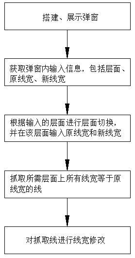
[0043] A method for modifying line width in batches in a kind of PCB board design of the present invention, described method comprises the following steps:

[0044] (1) Build and display pop-up windows;

[0045] (2) Obtain the input information in the pop-up window, including layer, original line width, and new line width;

[0046] (3) Switch the layer according to the layer input in step (2), and input the original line width and new line width at this layer;

[0047] (4) Grab all lines on the desired layer in step (3) whose line width is equal to the original line width;

[0048] (5) Modify the line width of the line captured in step (4).

Embodiment 2

[0050] A method for modifying line width in batches in a kind of PCB board design of the present invention, described method comprises the following steps:

[0051] (1) Build and display pop-up windows;

[0052] (2) Obtain the input information in the pop-up window, including layer, original line width, and new line width;

[0053] (3) Switch the layer according to the layer input in step (2), and input the original line width and new line width at this layer;

[0054] (4) Grab all lines on the desired layer in step (3) whose line width is equal to the original line width;

[0055] (5) Modify the line width of the line captured in step (4).

[0056] In step (1), building and displaying pop-up windows is a process of writing files and reading files. The software can recognize files in the above format, and call the above files to create display pop-up windows through proprietary functions; the content of the file is Pop-up window definition code, each control in the pop-up w...

Embodiment 3

[0063] A method for modifying line width in batches in a kind of PCB board design of the present invention, described method comprises the following steps:

[0064] (1) Build and display pop-up windows;

[0065](2) Obtain the input information in the pop-up window, including layer, original line width, and new line width;

[0066] (3) Switch the layer according to the layer input in step (2), and input the original line width and new line width at this layer;

[0067] (4) Grab all lines on the desired layer in step (3) whose line width is equal to the original line width;

[0068] (5) Modify the line width of the line captured in step (4).

[0069] In step (1), building and displaying pop-up windows is a process of writing files and reading files. The software can recognize files in the above format, and call the above files to create display pop-up windows through proprietary functions; the content of the file is Pop-up window definition code, each control in the pop-up wi...


PUM


Abstract

The invention discloses a method and system for modifying line widths in batches in PCB design, belongs to the technical field of PCB design, and aims solving the problem that the design efficiency islow as required lines cannot be rapidly searched, the required lines cannot be rapidly selected in batches or completely and the rapid modification of line widths cannot be realized in the prior art.The method comprises the following steps of: building and displaying a popup window; obtaining input information in the popup window, wherein the input information comprises a layer, an original linewidth and a new line width; carrying out layer switching according to the layer and inputting the original line width and the new line width at the layer; capturing all the lines, line widths of which are equal to the original line width, on the layer; and modifying the captured lines. The method and system are capable of rapidly searching required lines and rapidly selecting the required lines in batches or completely, so as to rapidly modify line widths and effectively improve the design efficiency.

Description

technical field [0001] The invention relates to the technical field of PCB board design, in particular to a method and system for modifying line width in batches in PCB board design. Background technique [0002] At present, there are a variety of PCB board (Printed Circuit Board printed circuit board) design software on the market. The most widely used circuit and layout software design tool in the industry launched by Cadence (an electronic design automation software company) not only has powerful functions It is supported by a variety of related software, and because it provides an open secondary development interface and a relatively complete development language library, users can develop according to their own needs. The skill language is a high-level programming language based on C language and LISP language built into the design software launched by Cadence company. The design software launched by Cadence company provides a wealth of interactive functions for the ski...

Claims


Application Information

Patent Timeline
Patent Type & Authority Applications(China)
IPC IPC(8): G06F17/50
CPCG06F30/392
Inventor 张敏
Owner ZHENGZHOU YUNHAI INFORMATION TECH CO LTD
Learn More